I've fallen in love with the art of creating beautiful, functional printed circuit boards. Filling in the copper, solder mask, and silkscreen layers, defining the edges of the boards, and even the weary time spent tweaking the sizes of different elements... It's so fulfilling!
I love that, once I finish the design, it's easy to order a bunch of them to give away to my friends and people I admire. And if I want to make a small change, it's the work of a moment – then after a little more waiting, I have the new version in my hands. It's truly magic, and I want to share it with you! So, I'm going to walk us through my process for creating PCB art with Procreate and KiCad, using three designs: my #Avnet100Years guitar pick, Companion Core, and "ESP-01" ESP8266 programmer board.
I picked up the KiCad side of this process from Andy Sowa, who walks us through it in the interview below. However, for this tutorial, I'll be showing you how I draw freehand art into the iPad app Procreate with a stylus, and convert that into layers for KiCad, an open-source PCB design application.
1. Choose a colorway and design the circuitThe first step is to decide what I want to include on the circuit, and where to put it. I design all the visuals around this. Often, I can move the parts around to form something beautiful – or place most of the traces on the back side of the board – but the specifics come later.
First, we need to know how it all connects together, and we do this in the Schematic Layout Editor (Eeschema). Here's my schematic for a simple, surface-mount LED circuit with a CR1220 battery and a switch, used in the #Avnet100Years guitar pick:
I use the SparkFun KiCad libraries for most component footprints.
Next, we decide what goes on the front/back, etc. – including components, routing, and design elements. Draw a rough sketch and imagine how all the parts will visually interact. Then, lay out a simple version in the "Pcbnew" PCB layout editor. We want to create our outline and route the circuit. We have a couple of options here:
- Design an SVG for the edges and use svgconvert to turn it into an Edge.Cuts layer (as for the guitar pick)
- Draw the outline by hand using KiCad's Polygon tool (as seen on the ESP-01 programmer) – In this case, I had already drawn a rough version of the board outline and imported it as a footprint, as you'll see below. I traced around that to create this polygon. I like the imperfection of this; along with the "chalk" silkscreen art, it adds a bit of rough-hewn, arcane charm.
It's important to consider your colors during the ideation and circuit design because, if we're using something like OSH Park's After Dark colorway, the copper traces will be visible under clear solder mask (or even coated in gold, if the solder mask is left off). Also, the base PCB substrate can be used as a color in itself – and it matters whether that is black or beige, and whether we get an extra color from the solder mask or it's clear.
2. Take a screenshot and send it to ProcreateIt's pretty easy to AirDrop files between my MacBook Pro and personal iPad. I take a screenshot of the whole circuit so far and pull it into Procreate, a popular art app that works well with the Apple Pencil stylus. I'll often make the bottom layer black, then put the screenshot on top of that at 50% opacity (so it isn't as dayglo-bright), and start drawing on top in white. If I were using a different colorway, I might set up the colors differently, but I'm pretty hooked on this one and the purple versions come out looking pretty cool anyway. :)
Here's a peek at each of the projects I mentioned, and the layers that went into them. For this first one, the layers show lots of trial and error, reference images, and a guide for the top text. I also have a layer with the embellishments for the back of the PCB.
One of the things I love about designing in Procreate is that you can use different brushes; for example, the Inka brush gives it a sort of "antique chalk" look that I really like:
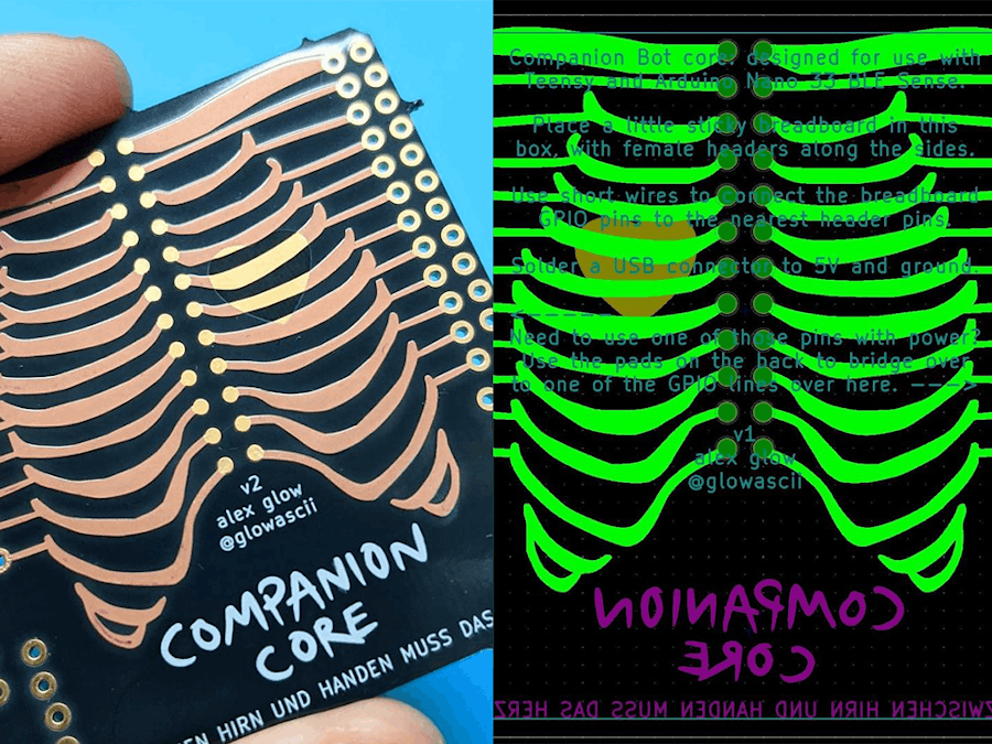
Now, here's the Companion Core:
And finally, here's the Avnet guitar pick, where you can see a couple of different designs I played around with before settling on the final one. There's a layer with the Starfire guitar head, which I used as a reference for the tuning pegs. The Avnet logo is traced from a reference image, using Procreate's tools to draw straight lines. (It's a Very Good app!!!)
Once it looks good, I export each circuit board layer as its own image, and AirDrop it back to the computer. Here are the two images I exported for the guitar pick, which would turn into silkscreen (white) and copper (gold) footprints:
There are a couple of things to note here:
1. The plus signs – These are fiducials / registration marks. They fall within the hole I made for connecting the PCB to earrings or keychains, so they don't show up on the final object. They just help me align the layers inside of KiCad. (I learned about fiducials while working at a screenprinting shop!)
2. File structure – Each of these images is an aggregate of several layers in Procreate, exported as a single.png graphic. For example, the strings are on one layer, with extra thickness added to the lower strings on another layer. The tuning pegs are on their own layer, too, but these all end up together in just one image.
Onto the computerUp until this point, all the graphical stuff has been kind of an arbitrary size – working from a screenshot and doodling on top. Now, we'll try to get it to the right size. There are probably better methods, but here's mine:
- Open the file in Preview.
- Crop it until the edges are at the image.
- Open Tools > Adjust Size... and set the resolution to 400 pixels/inch and the rough size you want it to be.
OK, here's where things get a little shifty. You can approximate the proper size for your image layers by looking at the image's size in pixels, and the resolution (dots per inch), so that it matches up to your PCB dimensions. Try to keep that in mind when you use KiCad's "Bitmap to Component Converter" tool. You can change the resolution a bit to get the right dimensions.
Editing the files: Once I hit "Export", I end up with a.kicad_mod file. As Andy taught me, we can open this up in a text editor to change the layer type. See how there's no Copper option under "Board Layer for Outline"? For copper, we'll need to pick a different layer type, and use Find & Replace to swap in "F.Cu" for "F.SilkS" or whatever we chose.
Side note: The above image is actually used on two different, identical, layers. First, I lay it down on the copper layer. Then, to get the gold ENIG coating, I use it to block the solder mask coating in the same areas. (Copper under clear solder mask stays copper.) So, it's actually the same.kicad_mod file, but with one version edited so it's on layer F.Cu and the other set up as F.Mask.
Side note: Another thing to note here is the "Negative" setting. It makes it a lot easier to generate files for your image on different layers:
- Copper (F.Cu): Black = applied, white = withheld
- Silkscreen (F.SilkS): Black = applied, white = withheld
- Solder mask (F.Mask): White = applied, black = withheld. (Black is shown in CAD, since by default, most of the board will be covered in solder mask.)
Thus, if you want to have the conductive layer show through, you can use a black-on-white image for both that layer and the solder mask. This will apply the copper and remove the solder mask above it.
Saving footprints: Once my.kicad_mod file is set up as the right layer, I'll use the "Footprint Editor" tool to import this file and save it as a footprint. I have one global library for each project's footprints, and a global library where I put the ones I use again and again – like the tiny Hackster logo. This is because I haven't yet gotten comfortable with KiCad's library system; ideally, each project would of course have a project library instead. (Uffdah.)
Adding footprints to the board layout: Next, I open up my board layout file in Pcbnew again, and use "Add footprints" to drop my new footprint onto the board. Hopefully, it fits pretty well! If the size is a bit off, at this stage I'll roll back to the bitmap converter tool and adjust the resolution a bit (higher DPI for a smaller image). At the sizes we're working, it shouldn't make a drastic difference in quality, but between 300 and 400 is still ideal.
The registration marks I used above are pretty helpful with aligning stuff. You can place them way off the edge, if you want to; just be aware that when you're dropping the footprint onto the board, KiCad will center its auto-scrolling on the cursor, so watch how you center the image in the Footprint Editor. If you're too zoomed in or the registration mark is way out, you may not be able to easily align it.
I'll be honest – this part can take for-e-verrrrr, and it's definitely not the most fun part of the process. But, look how pretty it becomes!!!!
I make liberal use of these hotkeys:
- F – flip the footprint to the other side (top/bottom) of the board
- R – rotate the footprint
- M – move the footprint
KiCad has a built-in text tool, as well, which you can use to make a self-documented board like the Companion Core above.
Once you get the hang of the layer colors (which you can choose), it's a bit easier to see where things sit in relation to each other. For example, the lime-green layers on the Companion Core are actually fully functional copper traces! They connect pins from one side of the board to the other, if you solder the jumpers in the middle.
If you need to do an extra check, KiCad also has a pretty sweet built-in 3D viewer, where you can set the colors as well:
I've gotten most of my art PCBs fabbed through OSH Park! I mostly use the After Dark colorway. You can order them here:
- Ouija 8266: project, PCB
- Joule Thief: project, PCB
- Avnet guitar pick: project, PCB
- Companion Core: project, PCB
- Purr Module: project, PCB
But if you want to order your own design, you can follow these guidelines to generate and upload the files.
...BONUS ROUND!Here's another one that I made for a "Purr Module" for companion bots (hosting four haptic vibration motors):
My friend had recently shown me how to use Procreate's symmetry tools, which are super helpful! The bees sit on the copper layer, and they're purely for style. They cost nothing extra! On a flex PCB like this, the copper shows up shiny gold if it's on the layer facing you (usually F.Cu), and black if it's on the layer facing away (B.C):


Comments
Please log in or sign up to comment.