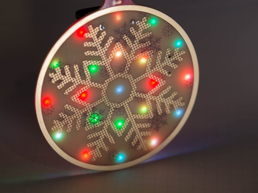
On November 24th I saw this tweet from @mrtwinkletwink:
I thought this was a really neat use of a 4-layer PCB in an artistic style! I started thinking about how you could design a PCB like this in KiCad.
One thing led to another and I'd ended up with a design ready to be sent off.
I double checked with JLCPCB about the manufacture of such a PCB. Often PCB companies may not like producing boards with lots of exposed copper areas on the front of the PCB. My contact at JLCPCB really loved the idea and sponsored this project! So I'm now left with many more PCBs than I would have otherwise bought, and in a BEAUTIFUL festive red colour.
There are a few different ways to get custom shapes into KiCad. You can use the built-in DXF import, or the Bitmap Converter. Additionally there are plugins for converting SVGs to KiCad PCB footprints.
I decided to use the DXF import feature, as this is the easiest IMO, it also handles scaling for you directly.
My plan was as follows:
- Design PCB shape in Rhino.
- Find vector style snowflake patterns online to import.
- Scale and export the snowflakes form Rhino into KiCad.
- Import PCB shape into edge layer.
- Import Snowflakes into footprints copper layer.
- Wire up LEDs in parallel to switch+batteries using only the back layer.
I had decided to use Rhino to perform all the 2d vector work and export DXF files, this could be done Inside KiCad but it's not really designed for it. I'm very familiar with Rhino for 2d vector work when laser-cutting. But there are other tools that can do this.
You're not limited to a simple circular shape for the outline of your PCBs. Most fab houses can take any shape you submit. Keep in mind that this outline is traced by a circular cutting bit, these are typically in the range of 1-2mm in diameter. This means any sharp interior corners will end up with a radius.
Once we have this outline in a DXF file we can import into KiCad as a Edge.Cuts layer.
On the front layer I wanted a more decorative snowflake pattern. I found this pattern by searching for "vector snowflake"
I decide to try out a feature in Rhino, "Hatch" to create a pattern inside of this outline. Hatch give you options for scale and rotation, adjust these to your liking. It is also possible to create your own custom pattern files in Rhino too.
I removed the outline and exported back to DXF for importing into KiCad again. In order to group the snowflake together we will make it a new footprint. So Open up the Footprint Editor and use the import DXF option.
KiCad does not allow you to import a DXF directly to a Copper Layer. So we have to hack the footprints with a text-editor after we have placed the pattern as we want it to appear.
Open up the exported footprint and change the layer definition for each line. (Use search and replace-all for this)
You can change this to any valid KiCad layer
- Front Copper - F.Cu
- Inner1 Copper - In1.Cu
- Inner2 Copper - In2.Cu
- Back Copper - B.Cu
- Back Silkscreen - B.Silk
Note after changing to an inner layer, it may not be visible in the footprint editor anymore. But the tracks will be visible in the PCB editor.
Do this step for each snowflake pattern you want on your PCB. I created some small/thin ones and also some larger/thicker ones for more variety.
With the artistic aspect taken care of the last step is the electronics. To be honest some projects may not even need this step! These look great even with the LEDs fitted.
ElectronicsThe electronics is made super simple by these LEDs with integrated colour cycling controller!
Here is the schematic for the circuit on the back. Can't get much simpler than that.
There isn't much too these. Solder on all the LEDs first, then the switch, then test everything works with the battery pack before soldering that in place.
Ensure polarity is correct when soldering down the LEDs.
The next artistic PCB I built will incorporate some changes/observations I've had from this design.
- The FR4 between Inner1 and Inner2 is too thick to see Inner2 from the front Side of the PCB.
- I'd place more snowflakes directly infront of the LEDs.
- Increase soldermask opening for LEDs to a larger rectangle.
Other than that I think these turned out great! I do have some spare PCBs.
I'll be selling a few kits on Tindie: https://www.tindie.com/products/15720/
I really want to see other peoples artistic PCBs! If you make one tag me on a photo of it on twitter! @GregDavill
These PCBs were sponsored by JLC. I've personally used JLC now for many projects and there boards are affordable, high quality, and deliver fast with DHL! If you have prototype PCB are small runs checkout their service at: https://jlcpcb.com/
Files/DownloadsAll design files are up on GitHub: https://github.com/gregdavill/xmas-led


Comments
Please log in or sign up to comment.