

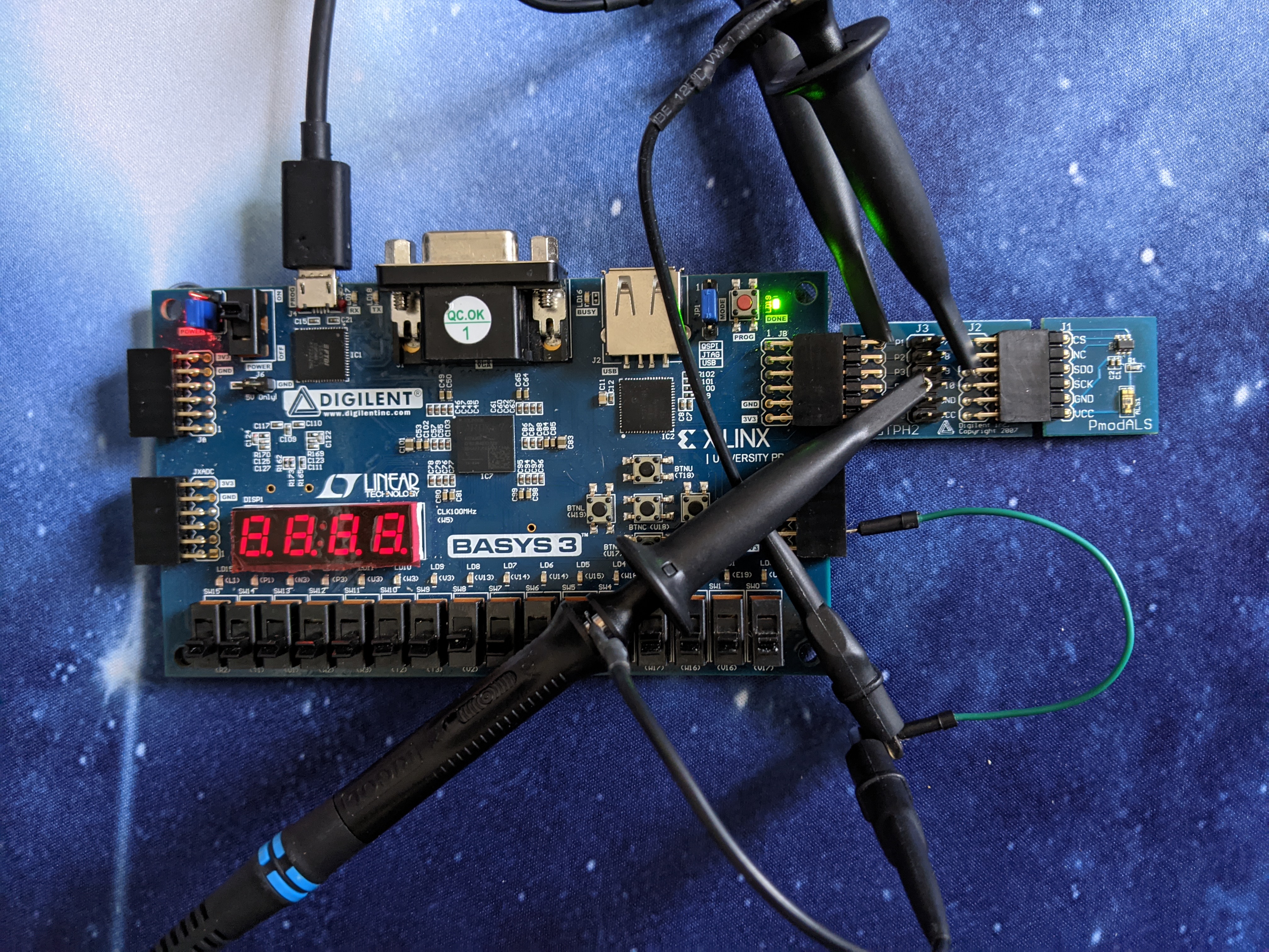
Hardware components | ||||||
 |
| × | 1 | |||
Software apps and online services | ||||||
| ||||||
Electronic hobbyists, makers, and engineering students need low-cost and effective tools. One of these tools includes a logic analyzer for debugging digital designs. Unfortunately, there is a large gap in this market, professional grade logic analyzers start at a minimum of 400 dollars while the cheaper version is around 15 dollars but is extremely limited in functionality. There are no mid-tier options that meet the needs of the aforementioned. This project is an open-source design using FPGAs offering great performance. In addition, the design uses only Verilog source code, no IP cores or device specific features. This makes the design portable to any FPGA, you can adjust the number of input channels and memory depth very quickly. For the accompanying desktop application, Python is used to allow the GUI to work on most operating system.
The following table summarizes resource utilization across various manufacturers. Xilinx FPGAs offer the best resource utilization when comparing to Alter and Lattice. Xilinx offers 6-input LUTs while Alter's and Lattice are 4-input LUTs.
DesignBreakdown
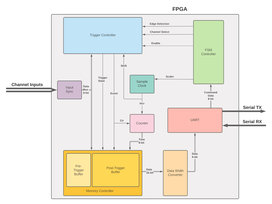
This project consists of 7 major blocks to carry out a functional logic analyzer: a trigger controller, sample rate counter, memory buffer, control module, and UART communication.
TriggerController
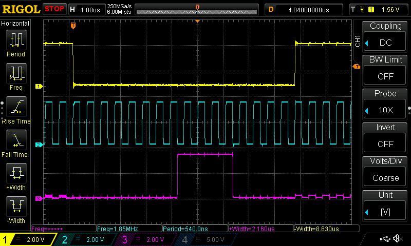
This module is set to wait for a trigger condition on a user configurable channel. That condition can be either a falling or rising edge and is set in the GUI. A sample rate signal is used to tell the trigger controller when to shift new input data in. If the new data does not match the current data, then an event signal is sent out to other blocks. Once the trigger condition occurs, a triggered state signal is sent to the memory buffer.
SampleRate Counter
This system takes in a 16-bit divisor that tells the logic analyzer what the sample frequency should be. The sample rate signal controls how often new data is shifted into the trigger controller and how often the timestamp counter should be incremented. This divisor is needed with the FPGA clock frequency, in the GUI, to derive timing information from the relative timestamps. The sample rate signal is a pulse lasting for one clock period of the FPGA system clock, the signal does not drive the clock of any connected blocks. This helps avoid crossing clock domains as all blocks run at the same frequency.
TimestampCounter
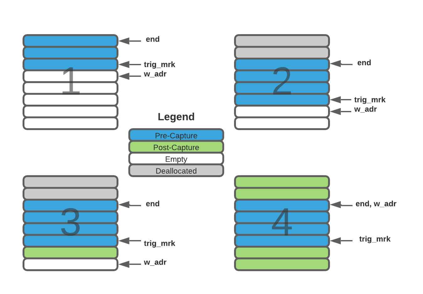
This system uses an 8-bit register to count the number of sample clock pulses. This register is concatenated together with the input data before being saved to the memory buffer. The timestamp counter is incremented at every sample clock to keep track of the relative time between events. If an event occurs the counter is reset to 1 and resumes counting. If the counter overflows, a signal is raised for the memory controller to start a new entry in the buffer. An enable signal is used to hold the counter at 1 until a capture has been started.
This system takes in a 16-bit divisor that tells the logic analyzer what the sample frequency should be. The sample rate signal controls how often new data is shifted into the
MemoryBuffer
The memory buffer combines the timestamp and data storing it in RAM. Each time it receives an event or timestamp rollover signal, a new row in the buffer is started. Before a trigger condition occurs, this block behaves as a circular buffer, continually overwriting previous entries. The size of this circular buffer is programmable in the GUI and is a ratio of the entire buffer from 10% to 90%. Once a trigger condition occurs, the buffer acts as a FIFO, filling the remaining memory up. Once full, the controller module is signaled, and data is read out row by row.
DataWidthConverter
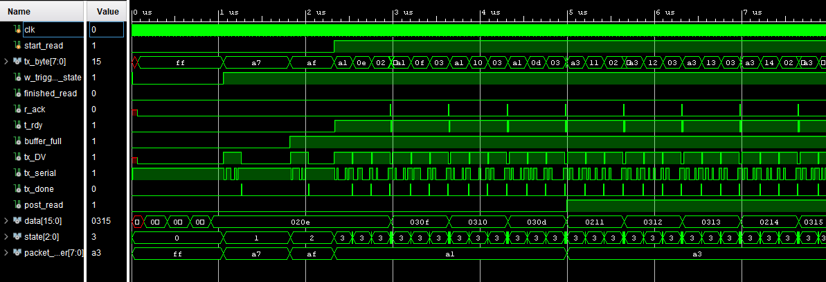
This block takes the width of the memory buffer data and converts it into 8-bit chunks so that the UART module can easily send data out. The data width converter also uses full-handshake protocol to securely transfer data from the memory buffer to the UART and to wait for the serial data to send before fetching the next entry. While it converts the width, it also prepends a header on the captured data indicating if it was captured before or after the trigger event.
FSMController
This block waits for commands to be received from the host computer and saves the commands to control registers. Once the enable command is received, the controller waits for the memory buffer to fill up. Then the data is read out of the buffer and converted from its original width to a width of one byte to be sent off to the UART block.
UARTCommunication
This block simply waits for bytes to be sent from the host PC and relays the commands to the controller block. This block is signaled from the data width converter when captured data is ready to be sent out. The BAUD rate of the serial data is set through a parameter called CLKS_PER_BIT and can be found by taking the FPGA clock frequency divided by the desired BAUD rate and then divided by 2 once more.
ResultsHowToUseTheGUI
Main menu capture buttons
- 1: Selects which channel to watch for a trigger condition.
- 2: Sets if the trigger type is a rising or falling edge.
- 3: Sets the ratio of data that will be before a trigger event.
- 4: Sets the sample rate, first number shows the sample interval rate, the next two numbers show the minimum and maximum record time respectively.
- 1: The channel name.
- 2: Indicates where the data came from. Is set to the filename if loaded from one or is Enxor if the data came directly from the logic analyzer.
- 3: The red bar indicates where the trigger point occured.
- 4: The position slider controls the x-axis. Click-and-drag to move the slider to a new location.
- 5: Time measurement with units. Click anywhere on the waveform and then click on a second point to show the time between the two points.
- 6: Indicates the status of the logic analyzer. The
READYstatus indicates that the logic analyzer is ready to start a capture. When the logic analyzer is enabled but has not triggered yet, the status will beWAITING. After a trigger event, the status will beTRIGGERED. If you stop a capture in the middle then the status will beSTOPPED.
_z71LRYaopa.png)


_z71LRYaopa.png)
Comments
Please log in or sign up to comment.