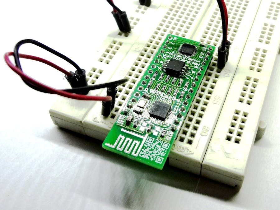
WiCard is a programmable WiFi module which connects to the user control panel or application via Wi-Fi. So It allows users to have access to its features over the air and wirelessly. WiCardTech group has designed the module as to not need a JTAG programmer after initial programming. Instead, WiCard modules can be programmed offline with the module’s hot spot, or online with a WiCard.Net account. The Integrated Development Environment (IDE) for this module resembles Visual Basic, which the programmers are most comfortable with, and the GUI and code generation can be accessed at the WiCard Simulator.
In the simulator, you can make a control box for the module, and have access to the module control box from the module hot spot (via the module’s Wi-Fi access point), the module IP (via port forwarding), and also the WiCard.Net account panel.
We created the module in such a way that it updates via WiCard.Net servers automatically.
ATMega8 - A 16 MHz microcontroller from AVR family (PCI Core)
ESP8266EX - High speed Wi-Fi controller and processor with Xtensa core
W25Q32F - 32 Megabit flash memory to save firmware and user program
The Wi-Fi core controls Wi-Fi transactions, reads the flash memory, and executes your programs. The PCI core controls peripheral components. Initial programming takes places with standard JTAG programmers. So for simplicity sake, we designed all subsequent firmware upgrades to take place wirelessly via WiCard's over-the-air (OTA) upgrade process.
In addition, the Xtensa core uses an external 26 MHz crystal and the AVR core has an internally configured oscillator.
WiCard Module and Pin ConfigurationThe WiCard module has 30 pins, including two 3.3 V VCCs, 2 GNDs, 22 GPIOs, 3 status LEDs, and one reserved pin for future features. Also the pins are in two 15-pin sides. So you can put this module at the center of a breadboard and use it for your different experiments.
The module has a 50Ω antenna located at the bottom of the PCB.
The figure below provides an overview of the pin configuration for the WiCard module.
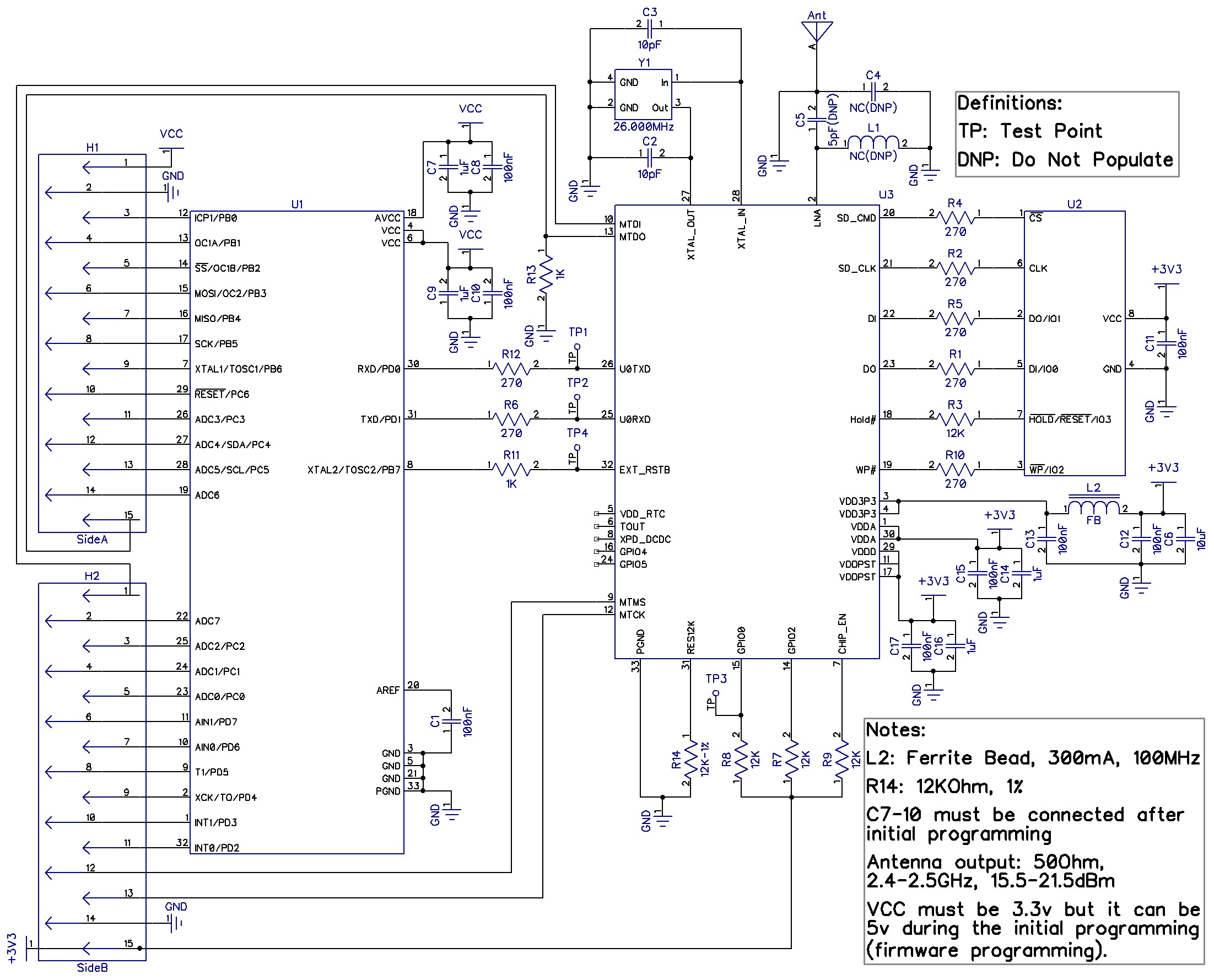
Our goal when designing the WiCard module was for it to be as straightforward as possible. In the end, we made it so the ESP8266EX connects to the W25Q32 and ATMega8A, and the ATMega8A microcontroller connects to the pin headers.
The resistor and capacitor values used in the schematic have been tested. So we recommend these values. However, you can make changes to component values and footprints for your custom PCB layout. (For example to simplify the production process.)
C5 and L1 form a matching network for the antenna and will vary from layout to layout. Based on the chip's stated impedance of (39+6j)Ω, a capacitive value of C5=0.7 pF and an inductive value of L1=1 nH provide a theoretical VSWR of 1:1 (0% reflected loss). A single 5-10pF series capacitor (inductor omitted entirely), provides a VSWR of 1.34:1 (~2% reflected loss). For the purpose of the initial experimentation, we made sure that the single capacitor sufficiently matched the impedance between the antenna and the chip which allowed 98% of the power from the chip to be transferred to the antenna.
In our production environment, C5 and L1 were determined experimentally with a network analyzer and applied to all identical boards.
PCB LayoutThe onboard antenna is a Meandered Inverted-F Antenna (MIFA). We chose this antenna because it has been designed for 2.4 GHz signals with 150-250 MHz bandwidth range on 20-60 mils (0.5-1.6 mm) thick, two-sided PCBs. The working distance of the onboard antenna of this module, is about 170 ft (50 m) in a closed area.
After assembling the parts on the PCB, program the initial firmware onto both of the cores. So making sure to program the ESP8266EX before the ATMega8A.
Programming the ESP8266EXFollow the standard steps of programming the ESP8266EX, which is with a USB-to-UART converter and the ESP Flash Download Tool, and used the following connections:
(Pin/Test Point --> Connect To)
B15 --> 3.3v Vcc
B14 --> GND
TP1 --> ESP Tx (COM port RX)
TP2 --> ESP Rx (COM port TX)
TP3 --> 220Ω Pull Down (to Ground)
TP4 --> 220Ω Pull Up Resistor (to +3.3V)
There are two approaches for programming the firmware on the module: the "WiCard specific programmer" created or a standard USB-to-UART programmer, such as the FT232RL FTDI USB to TTL Serial Adapter
Here's the standard settings for "ESP Flash Download Tool" for WiCard:
You can download all of the necessary files and the latest revision of the firmware from Trial.WiCard.Net .
The firmware for ESP8266EX includes 6 files:
- ESP8266EX_0x000000: Must upload it at address 0x0 in the 32Mbit flash memory. This file includes some initial system settings.
- ESP8266EX_0x001000: Must upload it at address 0x1000 in the 32Mbit flash memory. This file includes the firmware program data.
- ESP8266EX_0x0FE000: Must upload it at address 0xfe000 in the 32Mbit flash memory. This is a 4KB blank file for the system settings.
- ESP8266EX_0x300000: Must upload it at address 0x300000 in the 32Mbit flash memory. This file includes internal webpage data.
- ESP8266EX_0x3FC000: Must upload it at address 0x3fc000 in the 32Mbit flash memory. This file includes some initial wireless/WiFi settings.
- ESP8266EX_0x3FE000: Must upload it at address 0x3fe000 in the 32Mbit flash memory. This is a blank file for the system settings.
To programing the ATMega8A, use either an SPI programmer or a high voltage programmer (parallel programming mode). So for SPI mode, set the pins according to the following table:
A1 --> 5V Vcc
A2 --> GND
A6 --> MOSI
A7 --> MISO
A8 --> SCK
A9 --> XTAL1
A10 --> RESET#
Do not connect the other pins. Set the “Fuse High Byte” to 0xD8, the “Fuse Low Byte” to 0xA4, and the “Lock Bits Byte” to 0xFC. Also SPI programming requires pulling PIN A10 up (e.g., 10 kΩ) during use of the module.
Programming the module in high-voltage modeProgramming the module in high-voltage mode was different from programming in SPI mode. So for high voltage mode (parallel programming mode), Set the pins as shown below:
A1 --> 5V Vcc
A2 --> GND
A3 --> Data 0
A4 --> Data 1
A5 --> Data 2
A6 --> Data 3
A7 --> Data 4
A8 --> Data 5
A9 --> XTAL1
A10 --> Reset#
B3 --> BS2
B4 --> Data 7
B5 --> Data 6
B6 --> PAGEL
B7 --> XA1
B8 --> XA0
B9 --> BS1
B10 --> WR#
B11 --> OE#
TP 2 --> RDY/BSY#
Do not connect the other pins. Also C7, C8, C9, C10 somehow interfere with the high voltage programmer and need to be installed after the initial flash programming process.
Set the “Fuse High Byte” to 0x78, the “Fuse Low Byte” to 0xA4, and the “Lock Bits Byte” to 0xFC. There was no need to use a pull-up resistor for A10. Also this pin works as a normal input.
We designed the WiCard in such a way that programming the ATMega8A in the high voltage mode allows both the registration of new modules on the WiCard.Net servers and server access. Or, if users decide to go the route of SPI programming mode, We've made it so upgrading modules over the air and using all of the trial features is possible, except anything regarding pin A10, such as PCInt 7.
Circuit UseIt was important to us to make sure the WiCard module was suitable for industrial wireless control, IoT devices, home appliances, home automation, security systems, smart outlets and lights, infrared remote controllers, and sensor networks. This enables users to make products controllable by adding this module to existing circuits, thereby controlling a variety of devices via a computer or smartphone.
Programming and using this module requires only a stable 3.3 V power supply and a Wi-Fi compatible laptop, PC, or phone. The WiCard IDE software is still a work in progress. For now, if you're interested in giving the module a try, you can use the simulator page as the module compiler.
On that simulator page, there’s a compiler, a control box maker with some visual tools, and a WiCard simulator. A graphical user interface allows for programming without learning the underlying language, simply drag the items into the control box and edit the pin by double-clicking on the item.
You can compile your program in debug mode. So allows reprogramming of the module. Also with release mode, which requires a password to unlock and program the module. You can also use the module as a product controller (usually for public products). For a product controller, you simply need to compile in release mode so users won’t be able to edit or erase any of your other existing programs.
Here are the programming options:- Use a WiCard.Net account
- Upload the program via the module IP (port forwarding)
- Or upload the program via the router IP (offline)
- Also you can upload the program via IP address 192.168.4.1 (using the module Wi-Fi hot-spot to create an ad-hoc network)
- Export the program file and upload it to the module via the module internally hosted server page
After uploading the program, the module will execute and run the program automatically, and the control box is available in both the WiCard.Net account panel and the module's internal page. Registering the module and creating an account on the WiCard.Net server is not necessary for using and programming the module. The account simply provides server access and some extra features. The free version of the module will not connect to the server unless the user clicks on the "firmware update button" in the module internal page, which causes it to check for the latest free software revision to update. If you decide to connect to the server, the default password is "0123456789" .
ExampleThe schematic for the example project is simple. Pins A1 and B15 have been connected to the 3.3 V VCC, and pins A2 and B14 have been connected to GND. Pin A3 (port bit 0) has been connected to an LED with a 470 Ω series resistor.
The compiler will automatically generate the source code. The video below shows the WiCard in action.
DownloadDownload the schematics, PCB, Datasheet and the latest revision of WiCard Free Trial Firmware: https://trial.wicard.net/WiCard%20Free%20Trial.zip


Comments
Please log in or sign up to comment.