


I need a simple and cheap solution to scan TTL logic circuits at that time. So this is what I built.
The device has eight inputs and outputs and is connected to a computer via an LPT port.
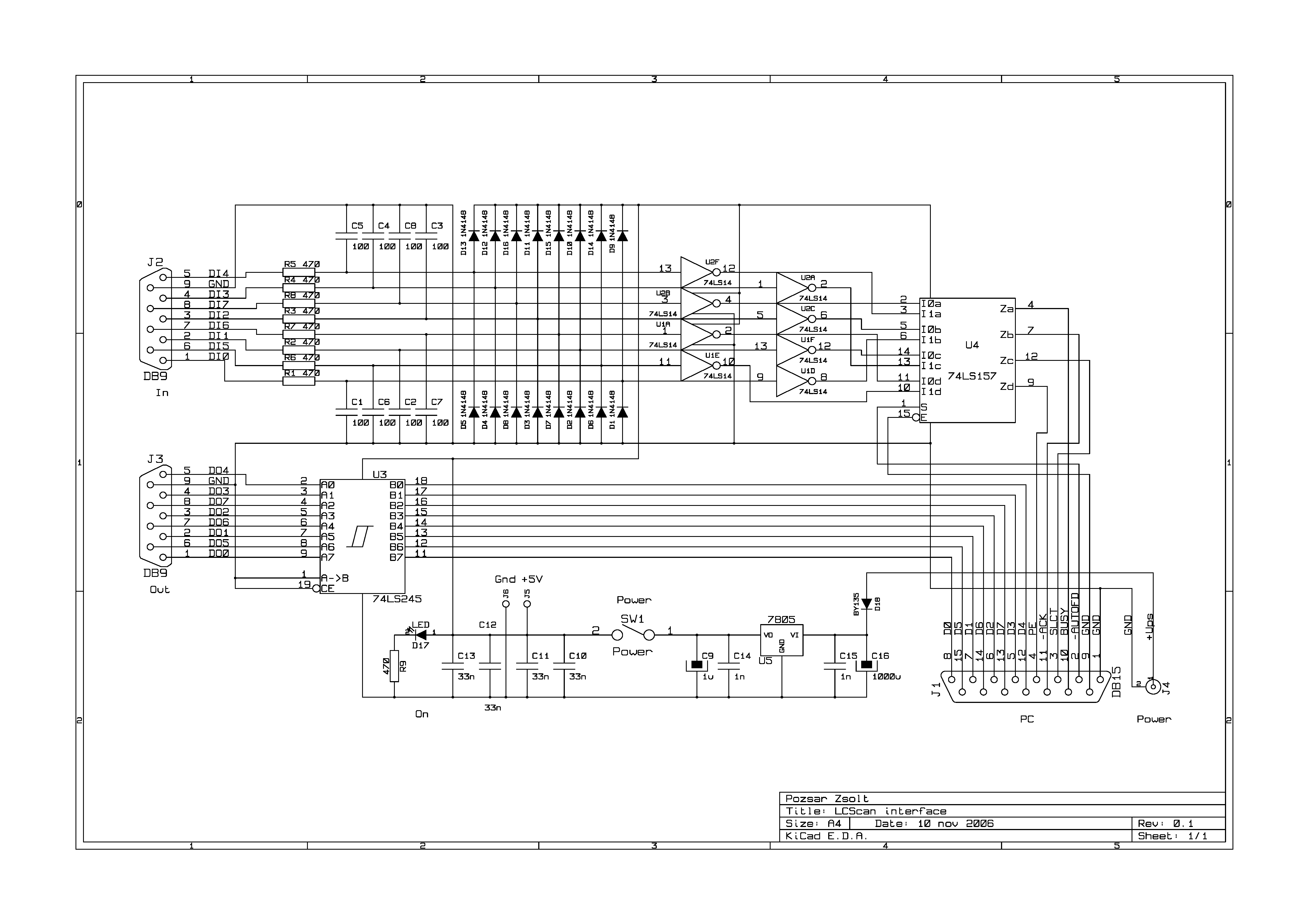
The input wires have limited over voltage protection. Inverting Schmitt-trigger circuits (2 pieces 74LS14) ensure the correct logic levels. PC reads eight bits in two parts using the 4x2 input multiplexer circuit (74LS157). The half-byte data is entered on the BUSY, -ACK, SLCT and PE lines, -AUTOFD is used to select the lower and upper half-byte.
The output is buffered with a bus transceiver (74LS245) circuit to protect the same circuit of the LPT adapter. The PC writes 1 byte data through lines D0-7.
The device works with a voltage of 8-12V DC (150 mA). The 7805 stabilizer integrated circuit produces the 5V power supply required by TTL circuits. This can also be found on the front of the device. A load of up to 800 mA can be connected to it.
You can find the schematic drawing in attached Github repository in KiCAD and Postscript format.
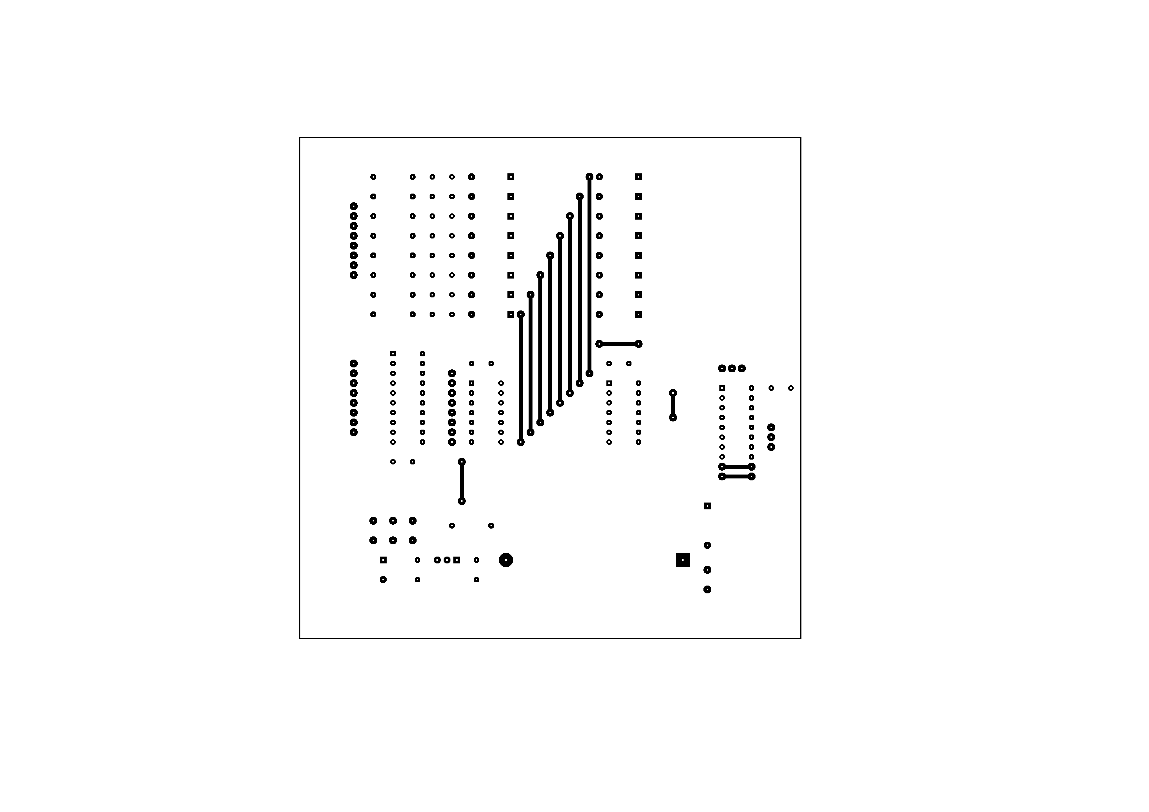
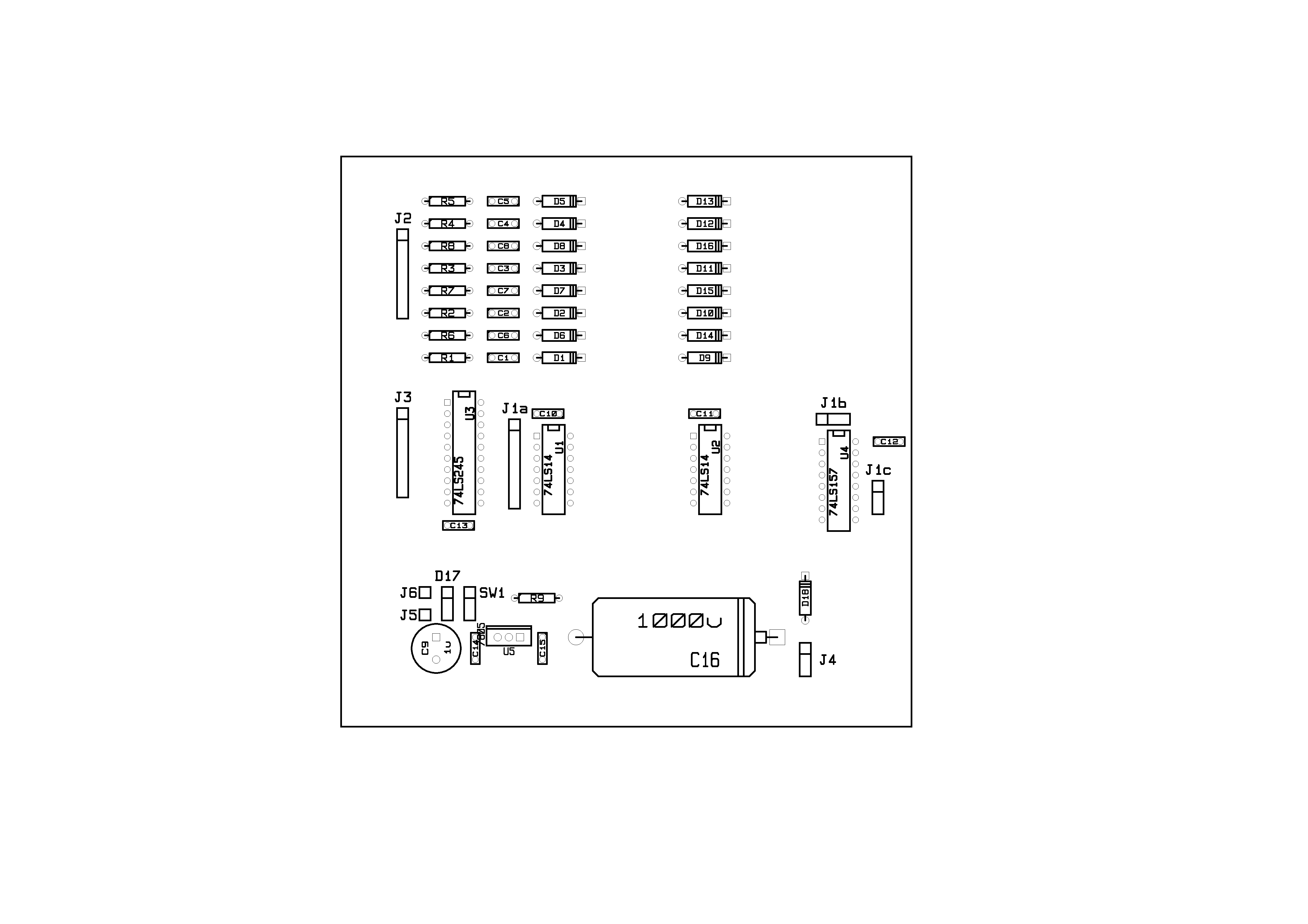
Printed circuit boardThe device was built from new and used parts found at home, so I used an old Soviet ceramic capacitor (green), a large, old Hungarian resistor (big gray) and an electrolytic capacitor (light blue), as well as a single-sided vinyl PCB instead of double-sided fiberglass.
You can find the drawings of PCB in attached Github repository in old KiCAD and Postscript format.
Internal cables and connectors
Between pc connector and board:
- 1: J6
- 2: J1b/1
- 3: J1c/1
- 4: J1c/3
- 5: J1a/2
- 6: J1a/4
- 7: J1a/6
- 8: J1a/8
- 9: J1b/3
- 10: J1b/2
- 11: J1c/2
- 12: J1a/1
- 13: J1a/3
- 14: J1a/5
- 15: J1a/7
Between in connector and board:
- 1: J2/8
- 2: J2/6
- 3: J2/4
- 4: J2/2
- 5: J2/1
- 6: J2/7
- 7: J2/5
- 8: J2/3
- 9: J6
- Between out connector and board:
- 1: J3/8
- 2: J3/6
- 3: J3/4
- 4: J3/2
- 5: J3/1
- 6: J3/7
- 7: J3/5
- 8: J3/3
- 9: J6
Between power connector and board:
- +U: J4/1
- GND: J4/2
Others:
- J5: to '+5 V' banana jack
- J6: to 'GND' banana jack
- D17: power on LED (1-Anode)
- SW1: power switch
The housing of the device is made from the housing of an old and wrong external modem (BEST 1414 EC).
The device comes with a plug-in power supply unit, a cable for the parallel port of the PC and two color-coded measuring leads.
Connecting the connectors
Cable between interface and PC (DB15-DB25):
- 1: 18-25
- 2: 14
- 3: 13
- 4: 12
- 5: 5
- 6: 4
- 7: 3
- 8: 2
- 9: 18-25
- 10: 11
- 11: 10
- 12: 6
- 13: 9
- 14: 8
- 15: 7
Colour-coded measuring leads (DB9):
- 1: white
- 2: yellow
- 3: orange
- 4: red
- 5: magenta:
- 6: green
- 7: blue
- 8: black
I always make programs that can be translated to several operating systems, but this is an exception. This is specially made for Linux only.
The program interface consists of 5 tabs: on the first one you can name outputs and inputs, on the second you can perform automatic scanning between two specified output values, on the third you can activate the outputs manually and monitor changes in the inputs. Here you can also see the color coding of the lines. The fourth tab is a binary/decimal/hexadecimal number converter. The fifth is the about page of the program.
The status line shows the address of the LPT port in hexadecimal and the value of the I/O lines in the binary, decimal and hexadecimal number system.
You can download source code from attached Github repository and binary packages from my hobby homepage. (The binary packages are very old, maybe need to be rebuilt.)


Comments
Please log in or sign up to comment.