


Hardware components | ||||||
| × | 1 | ||||
 |
| × | 1 | |||
 |
| × | 1 | |||
Software apps and online services | ||||||
| ||||||
Introduction to the MIPI CSI-2 protocol. The MIPI standard is not too difficult to understand so this project aims to give a good working example that can be up and running quickly. The project connects a Lattice Crosslink CSI-2 transmitter to a Jetson Nano CSI-2 receiver. The HDL files provided for the Crosslink imitate an IMX219 image sensor (CSI-2 output and I2C slave).
The project can also be used with a Raspberry Pi CSI-2 receiver as the lattice crosslink comes with a raspberry pi adapter in its kit. However, there are configurable parameters that I've added in the HDL that can used to replicate other image sensors.
The Nano and Pi come with built in IMX219 sensor drivers and is part of the device trees.
Project consists of 3 parts
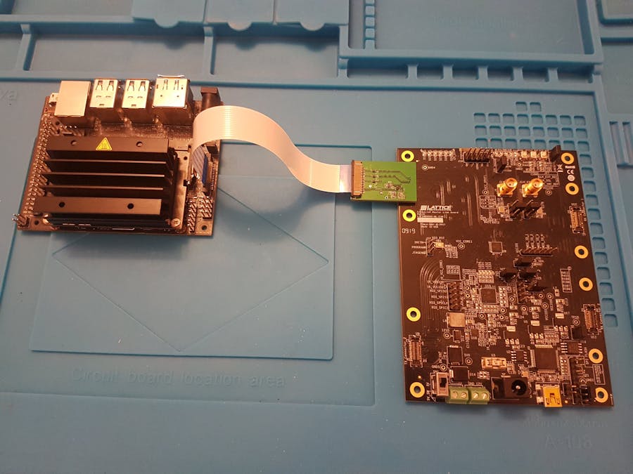
- Connector Board to connect the Crosslink board to the Jetson Nano.
- Verilog HDL code for Lattice Crosslink FPGA
- Jetson Nano to initiate streaming.
The connector board connects the FFC 15 cable from the Jetson Nano and maps 2 lanes of CSI-2 and I2C wires to the FX12B connector on the lattice board.
Board looked likes this
Code is broken into 3 parts
- I2C Slave
- CSI-2 Transmitter
- Image Generator
Some links to data sheetsIMX219 DatasheetCSI-2 Transmitter IP from LatticeAn older version of the MIPI CSI-2 Specification
I2C Slavei2c_slave_logic.v/i2c_slave_top.v
Slave_logic block is lattice source code that is controlled by the i2c_slave_top. The IMX219 i2c address is set to 0x10 and is set in slave_logic.
The i2c slave responds to the very few reads from Jetson Nano to what it thinks is an IMX219. The 3 registers that are read are shown below, the default values are just returned whenever they are read.
For writes from the Nano the i2c slave just acks all write commands and discards the information. The only exception is the register below which indicates if the CSI-2 stream should start or stop.
In order for the Nano CSI-2 receiver to operate correctly we have to imitate the image sensor specifications defined by the device tree. It has many modes I selected the one below. I removed some of the less important fields.
mode0 { /* IMX219_MODE_3264x2464_21FPS */
mclk_khz = "24000";
num_lanes = "2";
discontinuous_clk = "yes";
active_w = "3264";
active_h = "2464";
pixel_t = "bayer_rggb";
line_length = "3448";
pix_clk_hz = "182400000";
min_framerate = "2000000"; /* 2.0 fps */
max_framerate = "21000000"; /* 21.0 fps */
min_exp_time = "13"; /* us */
max_exp_time = "683709"; /* us */
embedded_metadata_height = "2";
};
First is to configure the CSI-2 Transmitter IP from lattice. You can use the attached data sheet for more details.
Settings can be seen below. Key components are non-continuous clock, the Tx Line Rate is equal to the pix_clk_hz. The reference clock is the built in onchip clock which is configured to 48Mhz.
In the files in the repository the '.sbx' file is created when the CSI-2 IP is generated with the below settings. It might not be enough to just copy that file into the project, you may have to generate it, as there are other background files created.
csi2_tx_simulation_ctrl.vThis code block is a large state machine to control all of the I/O signals in the block shown above. It sets up the small and large packet transmissions that are part of the MIPI standard. The settings of the data_type, word_count, virtual_channel and takes input from the image generator for pixel values and correctly times its transmission.
The code has some parameters within if other sensors, or other IMX219 modes want to be simulated. parameter NUM_OF_LINES = 12'd2464; This is actually the horizontal number of bytes to transmit per Tx lane. 3264 pixels * 10bit/pixel(Raw10) / 8bits /2 lanes
parameter ASSERT_BYTE_EN_TIMER = 12'd2040;parameter EXPOSURE_SIM_TIMER = 12'd3200; Simulating an exposure time is important for the device tree settings and making sure the FPS isn't too high.
When trying to compile the project the Input files should look like the following:
The '.lpf' file contains pin and IP info and needs to be copied from the Repo.
When compiling the project these are the settings to generate the bitfile.
The data transmitted over the CSI-2 transmitter needs to match the following from the IMX219 data sheet.
FS = short packet, frame startPH = long packet, packet headerFE = short packet, frame end
As per the device tree there are expected to be 2 lines of embedded data. The actual IMX219 places the internal register configurations in the embedded data lines.
However the simulator doesn't do that and outputs 2 lines of0x0A, 0x07, 0x07, 0x07, 0x55.0x0A being the embedded data (data type code), 0x07 indicating end of data and 0x55 a dummy byte which is needed in RAW10 mode.
For the pixel data the packet header data type is set to 0x2B (Raw10), virtual channel is always 0x0 and the word count increments per line. See the MIPI standard for more detail.
image_generator.vThis block generates images. Based on the line number and pixel number it programs the csi2_tx_simulator_ctrl block RGGB values. This outputs horizontal and vertical lines of differing colors on the screen.
If you don't have the devices and just want to learn the CSI-2 standard you can download the lattice diamond software and run the waveform simulator. There is a comment in simulator_top.v to do this.
Note there is any initialization time with the CSI-2 block, its about 50000ns before it can even think about starting to stream.
Before you boot up the Jetson Nano, the lattice crosslink board NEEDS to be connected and programmed. At bootup the Nano searches the I2C bus for connected image sensors from the list of image sensors. If it doesn't find anything at bootup you wont be able to launch the sensor (real or simulated).
If when you boot up these imx219 messages occur on the screen then you have issues.
When you have Nano booted up, open a terminal and runDISPLAY=:0.0 gst-launch-1.0 nvarguscamerasrc ! 'video/x-raw(memory:NVMM), width=3280, height=2464, format=(string)NV12, framerate=(fraction)20/1' ! nvoverlaysink -e
This will cause the Nano to write to the lattice to start streaming and hopefully images should appear on the screen.
The first image the the image_generator.v produces looks like this
Followed by some other images.
SchematicsYou can find the schematic which I did on EasyEDA here:https://oshwlab.com/daviesst/lattice-csi2-connection-board


Comments