


_4YUDWziWQ8.png?auto=compress%2Cformat&w=48&h=48&fit=fill&bg=ffffff)
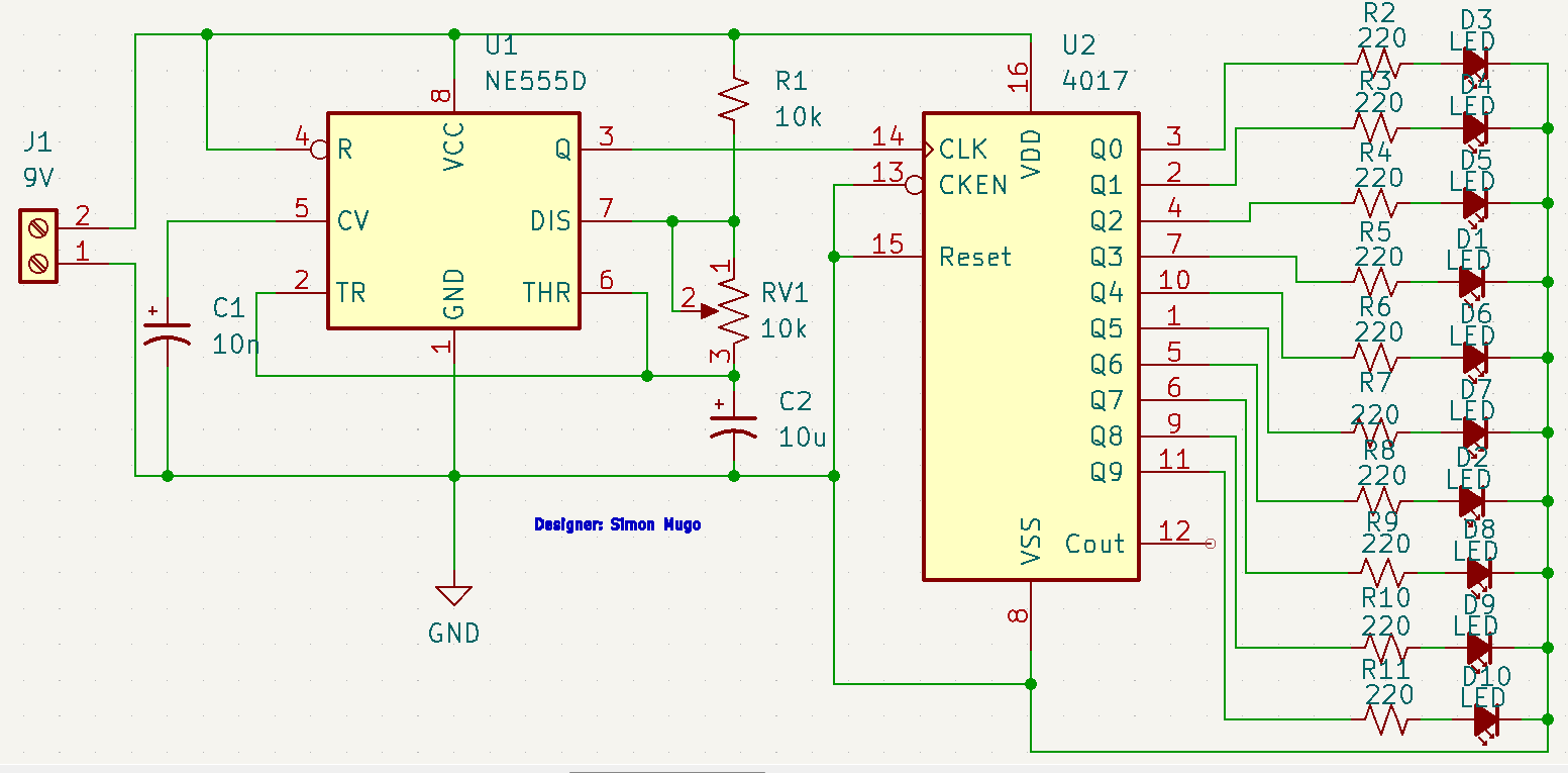
This project is to build NE555 IC LED Chaser Board, incorporating the 555 timer IC and the CD4017 IC. This electronic circuit can create a visually appealing and attractive effect where multiple LEDs light is sequentially illuminated. The illumination happens one after each another repetitively. The actual purpose is to create an illusion of a running or chasing light effect where the illuminating LED follows a certain array. Such boards are commonly used in signage, decorations, festive lighting, and display panels.
The project is made possible by the use of the 555 timers and CD4017 IC. The CD4017 is a decade counter-integrated circuit. The purpose of the 555 timer IC is the generation of the clock pulses and the CD4017 serves the purpose of dividing the frequency that it receives and also driving the connected LEDs.
This project directs the reader on how to do a simple LED chaser circuit with two main components: the 555 timers and the CD4017 ICs.
Project Required Components
NE555 timer IC
10 LEDs
CD4017 Decade Counter IC
10K Resistor -1
220 ohms resistor -10
10k Pot -1
10nF Capacitor
10uF Capacitor
Breadboard if you want to assemble it at home
Jumper wires
9V Power supply or Battery
Design of the Project CircuitThe circuit uses the KiCAD EDA tool, open-source software.
The circuit makes use of the NE555 timer IC as its driving force plus the CD4017 decade IC. Pin 1 of the 555 timers is the ground that connects the timer to the negative of the power supply. Pin 2 is the TRIGGER which a negative pulse on the pin sets the flip flop from a low to a high state. Pin 3 is the output that is used to drive any TTL circuit. Pin 4 is for reset which serves the purpose of resetting the internal flip flop hence controlling the status of the output. Pin 5 is the control voltage and its purpose is to control the 555 timer timing by overriding the 2/3 VCC level of the connected voltage divider. Pin 6 is the threshold that is connected to the positive input of the comparator and it resets the flip-flop when the voltage applied exceeds 2/3 of VCC triggering the output to switch from high to low. Pin 7 is the Discharge pin which is connected to the collector of the internal NPN transistor that is used to discharge the timing capacitor when the output at pin 3 goes low. Finally, pin 8, Supply + VCC is the power supply pin.
The timer is the driving force behind our Circuit.
The PCB LayoutBelow is the PCB layout done in KiCAD EDA.
PCBWay has an offer and sponsorships for the manufacturing of such and more projects. What you need to do is just send an email to PCBWay through sponsor@pcbway.com where your idea may be discounted or even fully sponsored into an actual final project. PCBway recognizes the efforts of the students and PCB electronic designers across the world and you just need a bold step to be one of the finest designers under them. Take the chance!


_Ujn5WoVOOu.png?auto=compress%2Cformat&w=40&h=40&fit=fillmax&bg=fff&dpr=2)


Comments
Please log in or sign up to comment.