https://www.hackster.io/Carlos_Diaz/new-nrf24-component-for-psocs-1f009d
Introduction
This component is based on a nRF24L01p library that I did some time ago, but using a SPI component plus some digital logic, now it is all wrapped into a PSoC custom component.
The Nordic Semiconductor nRF24L01P is a wireless transceiver that works on the ISM radio band. It is reliable and very easy to use. I got a couple of these modules on eBay for few bucks. Back then it was my first project using SPI on PSoC so it was a learning experience.
I had some problems with SPI implementation on PSoC. It is implemented on the UDB logic, and by default it has a Rx FIFO and Tx FIFO, both 4 bytes deep. So when you use that depth size the /SS line goes active automatically when it has a byte on the Tx FIFO (remember the /SS line on SPI is active low), and goes inactive (high) when it has no more data on the TX FIFO. It works like a charm, doesn't it?
Increasing the depth of FIFOsThings get a little difficult when you increase the depth of the FIFOs. The /SS line goes inactive even when you still have data on the TX FIFO, so with the help of the PSoC Developer Community I found out that I had to control the /SS pin manually in the software (with a Control Register).
But why increase the FIFO's depth? The nRF24 IC can send data packets up to 32 bytes in length, so if we want to send larger packets we need to increase the FIFO depth.
There's a lot of tutorials online explaining the nRF24 behavior, or you can read the datasheet to learn how it works. I prefer the second option complemented with reading about some similar projects online.
Component ConfigurationSo, we can see the component interns on the next image, a SPI component, a Digital Input pin with interrupt component attached to it, an a couple of Control Registers that controls /SS and CE signals.
Inside the SPI are the TX and RX FIFOs, both configured at a 32 byte depth.
The nRF24 internal interrupt is configured as default and it gets triggered on a falling edge. See the configuration below.
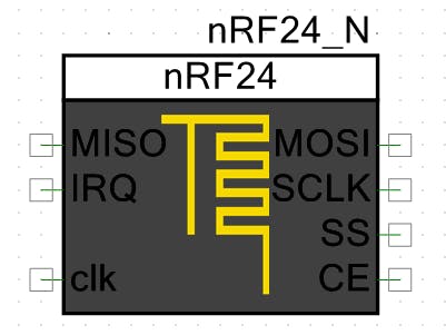
And the resulting component symbol is below.
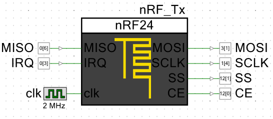
The component used on the test project bellow.
The clock in the component terminal will provide the clock to the SPI component inside, this clock must be twice the frequency we need the SCLK to run (SPI Clock), the nRF24 transceiver works up to 2Mbps, so the clk
input is connected to a 4MHz clock signal.
The pin connected to the IRQ input must be configured with a internal pull up resistor, and generate a interrupt in falling edges. See configuration below.
The example project do the following:
- Tx Side: First we need to create a new NRF_INIT_t variable, here we adjust the most common configurations for the radio, like the channel it will work on, if this radio is Transmitter or Receiver, the Data Rate, the Power, the number of times it will retry send a packet before give up and the time between those tries. After this i configure the Dynamic Payload feature using
x_WriteSingleRegister()function, with this function we can write to registers that are 1 byte wide. On the while loop it simply read a analog input with the ADC and save the result on the packet we will send to the receiver, it also save the number of times the switch button on the board has been pressed.
- Rx Side: This side is configured similarly to the Transmitter side, on the while loop it waits to receive the packet, then is transform the ADC result and button presses and print it on the console. Apart of this it reply the transceiver with a payload (saved on RXdata array).
This component accomplishes everything I need: very basic transfers. If you want to add other functions or behavior you can let me know or fork the GitHub repository, that's why I'm uploading it, to make it better with your help.
REMEMBER: nRF24 must be powered with 3.3v, pin inputs are 5v tolerant.
You can find the GitHub repository here.


Comments
Please log in or sign up to comment.