


Hardware components | ||||||
| × | 1 | ||||
 |
| × | 2 | |||
 |
| × | 1 | |||
 |
| × | 3 | |||
 |
| × | 1 | |||
 |
| × | 1 | |||
 |
| × | 1 | |||
 |
| × | 1 | |||
 |
| × | 2 | |||
| × | 1 | ||||
 |
| × | 1 | |||
 |
| × | 1 | |||
 |
| × | 3 | |||
 |
| × | 2 | |||
 |
| × | 1 | |||
 |
| × | 1 | |||
Software apps and online services | ||||||
 |
| |||||
 |
| |||||
Hand tools and fabrication machines | ||||||
 |
| |||||
After finishing my robot arm and Bluetooth car project, I realized I had used up all my available Arduinos. I didn't want to take apart my just completed projects to get the Arduinos back, so I started researching how to build my own. This would save money and give me a chance to learn and develop new skills, especially in PCB design.
You are expected to know how to use EasyEDA if you wish to replicate this project, the Gerber files are not provided.
For those interested, I have written theory for some of the non-essential components near the end of this document.
Project Requirements- The DIY Arduino had to be just as good as an Arduino UNO and be outfitted with features tailored specifically for my projects.
- It had to be cheaper than an Arduino UNO.
- All the parts had to be through hole and thus could be soldered on by me.
- It had to be reliable.
Specifications:
The ATMega328 is a single-chip microcontroller with a processor core architecture based on a modified version of the Harvard architecture 8-bit RISC. It has the following specifications:
- 1KB EEPROM (Electrically-Erasable-Programmable-Read-Only-Memory)
- 2KB SRAM (Static Random Access Memory)
- 23 GPIO pins (General Purpose Input/Output pins)
- 32KB ISP (In-System Programming) flash memory with read-while-write capabilities
- 3 flexible timer/counters
- Serial programmable USART
- SPI serial port
- Voltage rating of 1.8-5.5V
- 6-channel 10-bit A/D converter
Why is this chip used for the Arduino?
This chip offers high performance with low power consumption (typically 20-30mA), making it easy to power and convenient as a microcontroller. Additionally, it has a wide range of peripherals (pins) and is very easy to use and program, while still being relatively inexpensive.
Functions of each pin:
The ATMega328P-PU is the brains of our Arduino, responsible for processing and executing every instruction given through the Arduino IDE. It carries out these instructions through its peripherals/ pins. Therefore, it's crucial to understand what each pin on this chip does before attempting to make your own Arduino.
- Analog Pins (A1, A2,...): These pins convert analog signals from analog components to digital signals. For example, when using a potentiometer, the analog pin is connected to the potentiometer's output. The onboard ADC (Analog-to-Digital Converter) of the ATMega328P-PU compares the input voltage from the potentiometer with the output voltage at the analog pin to calculate the potential difference, and thus get a value that can be used.
- AREF (Analog Reference): When the Arduino takes an analog reading, it compares the voltage at the analog pin against the board’s reference voltage, which is typically 5V for an Arduino UNO. This means it can accurately measure voltages between 0 and 5V. The unit (in the IDE the
AnalogRead()function can return values from 0 to 1024) value returned byAnalogRead()corresponds to the reference voltage divided by 1024. If you need to measure voltages within a smaller range, like 0 to 3V, you can improve accuracy of the unit by changing the reference voltage. You can do this by supplying a voltage between 1.1V and 5V to the AREF pin. Make sure to use theAnalogReference(EXTERNAL)function in the IDE before anyAnalogRead()functions to avoid a short circuit. - Digital Pins (D1, D2,...)/GPIO(General Purpose Input/Output) pins: These pins control or read information from digital components connected to the chip. To turn on an LED, for instance, use the Arduino IDE to set the allocated digital pin as an OUTPUT pin and send a HIGH signal (equivalent to a binary 1). To turn it off, send a LOW signal (equivalent to a binary 0). Reading information from this pin is more software than hardware.
- OSC1/OSC2: These pins are for connecting an external oscillator, which acts as a clock for the chip.
- MISO (Master In Slave Out)/D12: This pin is used for the slave device to send data back to the master device in SPI communication.
- MOSI (Master Out Slave In)/D11: This pin is used for the master device to send data to the slave device in SPI communication.
- SPI (Serial Peripheral Interface)communication: Full-duplex, synchronous serial communication between one or more slave devices and a microcontroller.
- SCK (Serial Clock)/D13: This pin generates the clock pulses that synchronize data transmission between the chip and other components.
- RST (Reset): This pin resets the chip, similar to the reset button on a computer. The reset line is usually used when uploading code to the chip, signaling it to wipe the current instructions and make room for the new instructions.
- TX Pin (Transmit): This pin is responsible for transmitting data from the Arduino to another component. For example, a radio transmitter like the nRF24L01 is operated by the Arduino and sends out data transmitted by the operator to another Arduino.
- RX Pin (Receive): This pin is for receiving data from other components. For instance, a radio receiver like the nRF24L01 is operated by the Arduino and receives data from another Arduino, sending it to the operator for processing.
A little bit more on the RST pin:
The RESET pin is pretty unique compared to the other pins. Ignore the RST and DTR NetLabels for now; just think of the DTR label as an input signal.
So, why is there a 10k Ohm resistor there? It's a pull-up resistor. Let's break it down: if our RST pin isn’t connected to anything (essentially "off"), how will the program know if the pin’s state is high (connected to VCC) or low (connected to GND)? This uncertainty is called floating. To avoid this unknown state, we use a pull-up or pull-down resistor, which ensures the pin is either high or low while using very little current.
Since pull-ups are more common than pull-downs and relevant to us, we'll only focus on them for this project. Both work on the same principles, but a pull-up resistor connects to the high voltage (usually 3.3V-5V). For our chip, we need a 10, 000 Ohm resistor as specified by the manufacturer. By placing this resistor in series with the VCC, a small amount of voltage gets through, allowing the RST pin to stay in its LOW state and do nothing. Without the resistor, connecting VCC directly would keep the RST pin in a constant HIGH state, causing continuous resets, which isn't ideal.
But how does the chip reset during the upload operation to make room for new instructions? It's simple: when uploading the code, the computer also sends an instruction to the component responsible for converting serial data to TTL (Transistor-Transistor Logic) data to send a HIGH signal to the RST pin, bypassing the resistor. In this case, the DTR signal does the job. When this signal is received, the chip resets in synch with the data upload.
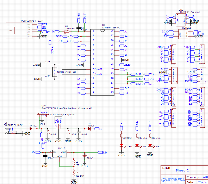
DESIGN: ATMega328P-PUAbove is the ATMega328P segment of the circuit diagram made in EasyEDA. We can see how each pin is effectively utilized and activated using the NetLabels from EasyEDA. How the GPIO pins and Analogue pins are used is very straightforward, so I won't get into it.
In the second image, you can see a 6-pin header. This header is used for burning the bootloader onto the chip. If you're replicating this design, make sure these pins are correctly connected and that you understand their orientation well.
Oscillator:
Note the 16MHz crystal oscillator connected to the OSC1 and OSC2 pins. Both pins of the oscillator are connected to ground and are in series with two 22pF capacitors.
A crystal oscillator is needed to provide a stable clock signal to the chip. The importance of this is to give the chip the ability to execute instructions in sync, otherwise the chip will simply not work due to the instructions being unable to adhere to the Von Neumann computer model.
FT232RL:
As you've probably noticed by now, the chip itself well, doesn't really have any integrated means to communicate with the Arduino, we need to add this. The circuit selected for this job was the FT232RL, which will act as our external Serial Port Module and translator for the chip. In simpler terms, we will use this to upload our code from the IDE.
The connection between the FT232RL and Arduino is established by linking the SPI (Serial Peripheral Interface) pins on the Arduino to the corresponding pins on the FT232RL. For transmitting data from the Arduino to the FT232RL, the TX (Transmit) pin on the Arduino is connected to the RX pin on the FT232RL, facilitating data reception by the FT232RL. Conversely, to receive data from the FT232RL, the RX pin on the Arduino is connected to the TX pin on the FT232RL, enabling data transmission from the FT232RL.
The DTR pin is connected in series with the RST pin, with a 0.1uF capacitor in between. This capacitor creates a brief reset pulse when the DTR pin is toggled, which is essential for resetting the microcontroller during code uploads. Without going into much detail, capacitors blocks low-frequency signals from passing through them and allow high-frequency signals to pass through. This setup helps ensure that noise or unintended signals do not accidentally reset the microcontroller. Additionally, the capacitor helps to improve the stability and smoothness of the reset signal.
DESIGN: Voltage RegulatorVin: Input voltage of the battery and DC Barrel Jack
FT3.3V: 3.3V output voltage of the FT232RL
3.3V Voltage Regulator:
The variable voltage regulator in this circuit was configured to output 3.3 volts by connecting two resistors in series to the Adj (adjust) pin of the LM317 voltage regulator. This regulator's versatility lies in its ability to be adapted for various applications and voltages simply by adjusting the resistance of the connected resistors at the Adj pin. In principle this voltage regulator works quite similarly to a linear voltage regulator.
Capacitors used are based on the recommended values from the component datasheets.
Formula for calculating the output voltage depending on the resistance:
5V Voltage Regulator:
Diodes in the circuit ensure one-way current flow, addressing the issue of multiple power sources. The last one prevents the 5-volt output from the FT232RL from flowing back through the 5-volt regulator circuit by acting as a barrier. This setup can be more clearly understood by observing the traces in the Gerber file and schematic. The first diode is to prevent any voltage from the 9V battery from interfering with the DC power jack.
Capacitors used are based on the recommended values from the component datasheets.
The PCBKeep in mind that when actually soldering the board, the LEDs and resistors for the RST and SCK were removed in the final circuit, due to the resistors changing the LOW and HIGH states of the pins, and hence not allowing a signal to pass through. Additionally, the resistors contributed to weakening the signals, resulting in any proper communication between the FT232R and the AtMega328-PU to be impossible.
Turning Schematics into a realityCompany used for manufacturing: https://jlcpcb.com/
Burning the Bootloader onto the ChipIt depends on where you order the chip from, but in my case, it didn't come with the bootloader pre-burned. After a lot of research and trial and error over two days, I figured out how to successfully burn the bootloader. Below is the method that worked for me. The chip absolutely needs the bootloader to function, as it's essentially the set of instructions the chip needs to know how to operate.
1. Connect any Arduino to your computer via the USB port cable.
2. Select your programmer board in Tools > Board, for example Tools > Board > Arduino AVR Boards > Arduino Uno.
3. Open up the Arduino IDE and then navigate to File > Examples > ArduinoISP > ArduinoISP
4. Once you have been sent to a new window titled “ArduinoISP”, ensure that the programmer being used is “ArduinoISP” and that you are connected to the correct port and board (board should be the master board and not the chip).
5. If you are then sure that everything is correct, compile and upload the sketch, which if successful should allow you to burn the bootloader onto the ATMega328
6. We can now start the burning process. It’s a good idea to enable verbose upload output in preferences since there will be no console output during the process otherwise. File > Preferences > Show verbose output during > Upload
7. Now wire up the ATMega328-PU to the master board as demonstrated in the image.
Or if the chip is already connected to the board use these headers:
Same connections, but make sure your orientation is correct.
8. When all the wires have been connected, connect the board to which the chip is connected to (Master board), to the computer (You may have to once more upload the code to the master board, as it tends to not save it after being disconnected)
9. To get the correct board, go to the board manager and install “MiniCore”. Additionally you may install it by going to file > preferences and inserting this link into the additional boards manager URLs: “https://mcudude.github.io/MiniCore/package_MCUdude_MiniCore_index.json”.
10. When you manage to install it, go to “select other board and port” and select the “ATMega328”
11. Change the programmer to “Arduino as ISP”, by going to tools > programmer > Arduino as ISP.
12. Ensure that the bootloader is: “Yes (UART0)”
13. Now burn the bootloader and wait for it to finish. If successful a window should pop up on the right stating that burning the bootloader was successful. However if you encounter an error, either check the connections between the chip and the Arduino or seek some help from the internet.
📖THEORETICAL INFORMATION PAST THIS POINTTHEORY: Voltage RegulatorsCapacitors: In a voltage regulator, capacitors are placed at the input and output terminals between VCC and ground (GND). Their primary functions include filtering out AC noise, suppressing rapid voltage changes, and improving feedback loop characteristics. Additionally, they serve as bulk energy storage, providing instantaneous voltage to the input or the load as needed. Capacitors are critical components in all voltage regulator circuits.
The output capacitor also serves another purpose: it acts as a temporary power supply to the load instead of the linear regulator. This helps prevent the output voltage from dropping when the regulator is adjusting to supply the increased current corresponding to the load's demand.
Pros and cons of using a ceramic and Tantalum capacitor, hence the variety of capacitors used for the voltage regulators.
Linear Voltage Regulator: The linear regulator employs an active (BJT or MOSFET) pass device (series or shunt) controlled by a high gain differential amplifier. It compares the output voltage with a precise reference voltage and adjusts the pass device to maintain a constant output voltage.
THEORY: Crystal OscillatorThe crystal oscillator circuit sustains oscillation by taking a voltage signal from the quartz resonator, amplifying it, and feeding it back to the resonator. A crystal oscillator relies on the slight change in shape of a quartz crystal under an electric field, a property known as inverse piezoelectricity. A voltage applied to the electrodes on the crystal causes it to change shape; when the voltage is removed, the crystal generates a small voltage as it elastically returns to its original shape. The quartz oscillates at a stable resonant frequency, behaving like an RLC circuit, but with a much higher Q factor (less energy loss on each cycle of oscillation). Once a quartz crystal is adjusted to a particular frequency (which is affected by the mass of electrodes attached to the crystal, the orientation of the crystal, temperature and other factors), it maintains that frequency with high stability.
What’s the purpose of those two capacitors? Well, they actually play quite an interesting role. Inside the chip, there's a signal amplifier, and the positive feedback loop is completed through the crystal. A positive feedback loop in electronics is a type of feedback mechanism where the output signal is fed back into the input, but with the same polarity as the original input signal. This results in an amplification of the original signal, leading to an increase in the overall gain of the system.
The crystal ensures that any signal passing through resonates at the resonant frequency, giving the strongest signal strength. However, the crystal can vibrate in several modes, leading to multiple resonant frequencies. While the fundamental frequency gives the greatest signal strength, harmonic frequencies can also create peak gains.
Natural stray capacitance would reduce the gain at high frequencies, but if the amplifier gain is high, we can’t rule out the possibility of the loop gain exceeding unity at these harmonic frequencies. In this situation, the oscillator might get locked into 3X or 5X frequencies, causing havoc with the digital circuitry. The addition of the two capacitors reduces the loop gain for higher frequencies, ensuring the oscillator oscillates at the fundamental frequency. Remember, capacitors allow high-frequency signals to pass through to the ground, attenuating them.
THEORY: FT232RLThe FT232RL Module derives its name from its core chip, the FT232, boasting an impressive array of functionalities. Among its capabilities, it excels in converting serial data from USB to TTL (Transistor-to-transistor logic), and can conveniently regulate voltage from USB to 5V and 3.3V. Remarkably, this chip operates without the need for any external hardware or firmware.
One of the key components of the FT232 is the UART Controller, which block converts the USB data format so that it can be sent over the UART (universal asynchronous receiver / transmitter) data lines RX and TX. This controller is programmable in FT232 IC to make the CBUS and DBUS pins (TXD, RXD, RTS, CTS, DTR, DSR, DCD, RI) pins to function as normal GPIO pins. By factory default these pins will function as control pins for USB to UART communication.
Interesting to note as well that the FT232 does not have a SCK pin, which is due to the way USB works. SPI doesn't need any 'Baud' (a unit of transmission speed equal to the number of times a signal changes state per second. For signals with only two possible states one baud is equivalent to one bit per second.) rate since it is a synchronous protocol.
DTR and RTS: Unlike RXD and TXD pins that are used for sending and receiving data, RTS (Request To Send) and DTR (Data Terminal Ready) pins are used for signaling purposes. In this case the microcontroller programmer uses the DTR line of the PC serial port to reset the microcontroller during the programming operation.


_3u05Tpwasz.png?auto=compress%2Cformat&w=40&h=40&fit=fillmax&bg=fff&dpr=2)
Comments