(This project is being managed here: Project Repository )
Description:This PCB design board is useful for the RF signals to determine the strength of the signals and the range of transmitting signals. This meter receives the signals and tells the user to improve or adjust the gain if required. This can detect the RF signals within the wideband frequency range. This can also be referred to as the field strength meter of the RF detector for wideband.
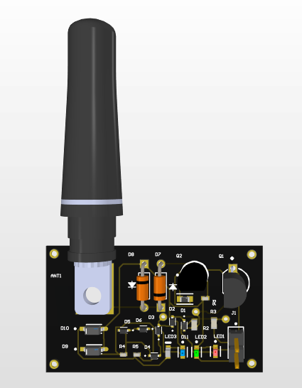
RF Field Strength Meter with Attenuator up to 200 MHz
The field strength meter is used to measure the radiation intensity from a transmitting antenna at a given location. With its own small antenna, it is essentially a simple receiver with an indicator. It measures the electric field strength emitting from a transmitter.
This board works on an operating voltage of 12V. There are four major LEDs attached to a board; yellow for low signals, blue for medium signals, green for high signals, and red for full signal indication. Using this PCB board you can improve the gain and the quality of signals.
Yellow LED for low signal indication
Blue LED for medium signal indication
Green LED for high signal indication
Red LED for full signal indication
The designing of symbols and footprints of the used components is an important step in PCB designing. After creating the symbols and footprints I have uploaded libraries which include the schematic and PCB library online on Inventhub. Those who want to implement my design do not need to redesign their parts, instead, they can download them from my collection and can reuse them. Moreover, I have attached the supply chain link of each part which allows users to find the availability and pricing of the component.
Schematic Diagram:I have designed my schematic in Altium designer. After completing my layout, I have uploaded my schematic file online on Inventhub. Those who want to implement my design can download the schematic without any error. I can also view the changes I have made in my design by going to the ‘view changes’ tab. I can also collaborate with the people, they can comment on my design and can give suggestions to improve my design further.
PCB Design:After completing my schematic design, I have converted it into the PCB file in Altium, where I can create connections on the board, define the shape of the board, arrange the components on the board, and can view my PCB in 3D view. I have uploaded my PCB file on Inventhub, where I can view my boards in different layers and can focus on a specific layer by disabling the other layers. Users and manufacturers can easily view or download my design for implementation.
Design for Manufacturing:For the fabrication, I have created a release file of the project on Inventhub which contains all the design files like Schematic, PCB, and Gerber files in a ZIP file format. Instead of visiting my manufacturer, I can send him the release file of the project. He can easily download the files and can fabricate my PCB board without any error.
Bill of Materials:I created a list of components on Inventhub which contains the details of the manufacturer, supplier, manufacturer part number, pricing, and quantity. By just putting these details in the BOM file on Inventhub, I can easily calculate the total cost of my project automatically using the supply chain option. My total cost for this project is $9.560. I can also view the datasheet of the component and can view its 3D model. Instead of visiting the component provider, I can send him this BOM file, he can download it in CSV file format and can deliver my components as per my design requirements.


Comments
Please log in or sign up to comment.