


(Geeks shall directly jump to the Challenge and Existing Solutions section)
Design and deployment of (self-made) IoT systems for monitoring various ambient and weather conditions (temperature, humidity, pressure, light, rain, gasses, motion) have become one of the most popular projects that every (starting) hobbyist has done at least once in a lifetime. The availability of hardware building blocks from OEM and DIY kits providers, as well as a plethora of free software (open source, ready-made solutions, libraries, drivers, IDEs, applications, OSes, cloud middleware, etc.), have made such projects pure no-brainers. The role of a designer is usually reduced to only picking the right sensor modules that are attached to a "beefy" MCU board (ESP32, Raspberry, Arduino), gluing existing software (drivers, libs) together, and programming a simple application logic. Not to mention a myriad of guidelines, blogs, and YouTube tutorials.
This approach has many advantages such as rapid prototyping, no need for deep knowledge and experience, great fun, a lot of support, and no (or significantly reduced) frustrations. For those few who decide to go further with the project and want to build and deploy plenty of sensors in/around their property, or go even commercial (at least selling the solution to your friends or family), this approach has several drawbacks. The most significant one is the overall price of the solution (and lower margin if you sell it). Indeed, it is perhaps cheaper than over-priced products from well-known brands. However, using ESP32 (dual-core 32-bit @ 160 or 240MHz, 320 KiB RAM, 448 KiB ROM CPU with a huge number of IOs and busses) is an overkill to fetch a few bytes from notoriously used sensors (e.g. DHT11, DHT22, DS18B20, AM2320, BMP280) over SPI/I2C/one-wire busses. Besides that, using Wi-Fi to forward a couple of bytes to a central hub (another ESP32 or Raspberry) has nothing to do with (energy) efficiency. Bluetooth low-energy (BTE) profile can be an improvement, however, the price of the module (e.g. HC-05) is multiple times more expensive than MCU itself including some sensors.
To sum up, there are two main non-functional requirements for small IoT sensors:
- Cost optimization: Due to large quantities, the production shall be economical. Thus, IoT sensors should be small in size (PCB), based on low-end and low-cost MCUs (to maximize utilization of resources), and use cheap connectivity for remote access. Low-end MCUs have a small pin count which is good for PCB optimization but it limits the number of attached IO devices/sensors. Furthermore, low-end MCUs have scarce resources (flash, RAM, IO, buses) which limit overall functionality (application and requires SW bit-banging for IO protocols). Nevertheless, IoT sensors typically collect only a few environmental properties (2, perhaps 3). This does not require to use of a large number of pins and MCU resources.
- Easy deployment and autonomy: Sensors shall be easily re-deployed (attached) without a need for changes in its surrounding and environment. There should be no need to additionally install wires to provide power and communication to sensors, i.e. sensors shall be wireless and battery-powered (or capable of extracting energy from the environment). Therefore, such sensors (incl. communication modules) are required to be ultra-low-powered (nano to microampere range) to avoid frequent battery replacements.
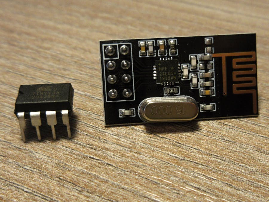
For communication modules, there are several COTS options that satisfy both low-cost and ultra-low-power needs. One of them is transceiver nRF24L01+, which is particularly popular among makers and hobbyists. It has a low price (breakout boards on Chinese webshops from 0.8 USD) and ultra-low consumption (990nA in power-down mode, 22uA in stand-by, and 12mA during TX/RX with max power). Furthermore, it has a simple interface (SPI with 5V tolerant logic pins despite being a 3.3V powered device), many favorable features (e.g. ISM band 2.4GHz with a range from 100 up to 1000m, 0.5-1-2 Mbps bandwidth, auto-retransmit, auto CRC check, multiciever), plenty of cheap (breakout) modules (see below), and several SW libraries (nRF24 for Arduino/Raspberry Linux).
Typical low-end(-cost) MCUs popular among hobbyists is 8-bit AVR subfamily with the limited peripheral set called ATtiny, specifically 8-pin 25/45/85 and 14-pin 24/44/84 versions (the first digit is the flash size in KiB). Arduino's 28-pin ATmega328P belongs to the family of ATmega with an extensive peripheral and instruction set. It offers 32KiB flash with 4x greater RAM, more IO devices, and is more expensive. In situations where (PCB) size, low-pin count, and cost do matter a lot, ATtiny series 25/45/85 and 24/44/84 might be preferable to 328P.
Another interesting low-end MCU is 8-pin ATtiny13A with 1KiB flash and 64B SRAM. It is 2-4 times cheaper (< $1 ) and consumes less energy than 25/45/85 and 24/44/84 ATtiny series. Thus, it is particularly popular in small, simple, battery-powered low-cost designs (what most of the wireless sensors are).
Combining ATtiny13A with the low-power wireless module nRF24L01+ appears to be a feasible choice for IoT sensors covering the above-mentioned non-functional requirements.
Another reason why someone would bother to fit nRF24L01+ on 8-pins minuscule ATtiny13A with 1 KiB flash which already has 3 pins occupied by sensors in an ultra-low-powered device is... just to have a good time, laugh, and great fun because:
"In 2K, you barely have room to brush your teeth."Challenge and Existing Solutions
- Joe Decuir
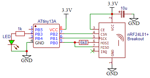
The combination of low-end 8-pins ATtiny13A with nRF24L01 is not a trivial task due to both hardware and software challenges. In our review for generic 8-pins MCUs, we described both HW and SW challenges of the marriage in greater detail. To recall, the hardware challenge is shown in the following figure:
ATtiny13A has practically available 5 pins. In case we reprogram PB5 from its primary functionality (RESET/dWIRE) to the IO port, we have 6 pins. However, the use of all 6-pins requires high-voltage programming. This is not always feasible for In-Circuit Serial Programming (ICSP). Furthermore, we do not have any spare pins for interfacing sensors or connecting to a fieldbus. From reviewed existing solutions, all HW proposals are in principle applicable for ATtiny13A but each has an associated "cost":
- Ralph's 2- and 3-pins solutions require several additional passive components. Pulling CE permanently high will not allow to fully exploit power-saving capabilities of the nRF24 module. Thus, it is not an ideal solution for ultra-low-powered applications.
- Not using IRQ signal will release 1-pin (e.g. PB5) which can be used for its primary functionality (RST/dWIRE) but we are still not able to connect other devices.
- Shared CE pin is not a generic solution. It will not interfere with the module when CSN is low. However, it might not be compatible with any attached device(s) or fieldbuses when used to control nRF24.
- Uni-directional SPI is applicable in wireless sensor networks (WSNs) which have one-way (simplex) communication to the main gateway. Thus, this is not a generic solution but works with a certain type of WSNs.
Unfortunately, not every reviewed SW solutions have a sufficiently low memory footprint and/or support all features:
- nRF driver for Arduino and RPi has an optimized fork for the ATtiny sub-family. The fork is still large and cannot fit even to ATtiny2313A that has twice as much memory as t13a.
- Nerd Ralp ported tinkerer.eu library that is tailored for ATtiny84 (8KiB flash, 14-pins) to his ATtiny85 (8KiB flash). It is not clear what is the overall footprint and whether it fits into 1KiB flash. Furthermore, the library relies on Universal Serial Interface (USI) peripheral that is not presented in t13a series. This can be fixed with a bit-banging.
- This particular shared CE pin solution runs on t13a and SW driver for nRF24 is a stripped-down Mirf library and it supports only transmissions (despite the fact it requires bi-directional SPI with MOSI and MISO signals).
To sum up: all listed HW solutions optimize only one parameter - the pin count. None of them optimizes 1) energy consumption, 2) pin count, and 3) code footprint at the same time. This is critical for ultra-low-power applications. Moreover, there is a lack of a proper SW driver that supports half-duplex wireless communication which can fit into t13a as well as supports some of the pin-count optimization solutions. We believe there is room for further improvement. For this reason, we have devised a completely new SW library described in the rest of the text. The library supports three HW configurations described separately below:
- Shared CE and CSN signals - it can be standalone or combined with the remaining two configurations.
- 3-wire SPI (merging MISO and MOSI),
- optional uni-directional SPI (no MISO).
Both CE and CSN are input pins and according to the nRF24 product specification:
- CSN is chip select and is active low. Pulse (low-high-low) duration of at least 50ns is required to indicate the start of a new transaction on SPI (page 49 in the spec, Figure 25 and parameter Tcwh, Tables 18-25). If we keep CSN down but we will not provide a clock signal (CSK), no data will flow and the module will not receive any command. Thus, nRF24 will stay in its current state and internal registers will not be affected.
- CE is used to activate the chip in RX or TX mode and is active high. To switch the module's radio into TX or RX mode, a pulse of a minimum of 10us is required (Sec. 6.1.5 on page 22 and Figure 13 on page 40).
From this we can identify the following conditions with shared CE/CSN signal:
1) CE/CSN is LOW, no pulses on SCK: Default case, radio not enabled, nRF24 not affected.
2) CE/CSN is LOW, the clock signal on SCK: Data transfer between MCU and nRF module via SPI.
3) Pulse on CE/CSN greater than 50ns and smaller than 10us: Resets SPI interface and indicates the start of a new transaction.
4) Pulse on CE/CSN for 10us: Enables radio mode (TX or RX) if the module was previously is in the StandBy-1 mode (activated by setting PWR_UP bit in the config register via SPI interface).
5) Pull CE/CSN high for more than 10us: Used in RX mode to wait for new messages.
We will use condition (1) CE/CSN is low as the default state on the signal. The selection of whether we want to enable/disable the radio (normally controlled by CE) or to read/write registers via SPI (normally controlled by CSN) will be "encoded" with different pulse duration.
In case we want to perform a transaction on SPI (accessing control/status registers and TX/RX data buffers) the procedure will take the following steps:
- 1 -> 3 -> 2 -> 1.
To enable a radio let us firstly look at TX mode. Before we switch to TX mode we have to properly configure the nRF24 module (powering up, entering StandBy-1 mode) and upload data into TX buffer(s). This is done with regular SPI transactions and steps described above. Afterward, the procedure to trigger transmission will take the following steps:
- 1 -> 4 -> 1
The module will switch to the TX mode, will perform all operations (transmission, waiting for acknowledge, retransmissions, timeouts) and after all TX buffers are empty will switch back into the StandBy-1 mode because CE is low. If we keep CE high all the time, even after buffers are empty, the module would enter into the StandBy-2 state. The difference is in the power consumption: 22uA vs. 320uA, i.e. 15 times greater in StandBy-2. Such power consumption is equal to ATtiny13A at 1MHz in full active state. The module will stay in the StandBy-1 until MCU pool the nRF24 for the state and eventually power off the radio (PWR_UP=0 bit), i.e. switching into the PowerDown state that consumes only 990nA. This short pulse on CE saves some energy which in ultra-low-power applications does matter.
The situation for receiving (RX mode) is slightly different because we have to wait for a relatively long period of time to receive some data. To perform a short pulse on CE/CSN of 10us will not be sufficient. One option is to keep CE/CSN high for a desired period of time. During this period we cannot access nRF24 with SPI. This issue can be mitigated by setting a sufficient amount of re-transmissions, timeouts, and message acknowledgment properties on the transmitter side. It should be configured that duration of the SPI transaction to read a status register is shorter than the entire transmission session (including re-transmissions). The procedure will take the following steps:
- 1 -> 5 -> 1
This solution works well for devices primarily used for transmission and is less effective for situations when the device is expected to be permanently in the receiver mode. For such situations, it might be more efficient to not merge CE and CSN. Instead, pulling CE to Vcc (high) would allow ATtiny13A to pool for new messages without a need to switch off the radio.
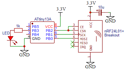
Config 2: 3-wire SPIThe idea is to merge both SPI data signals MOSI and MISO into a single one via a resistor as shown in the following figure:
This is not a new idea and is relatively common in various designs to reduce the number of signals. Will the nRF24 module work correctly with such a signal merge? In this figure is shown SPI communication with the nRF24 module from the documentation:
We see that nRF24 uses MISO to send the status byte while the master (MCU) sends a command to the module, i.e. full-duplex communication. Afterward, the MISO line goes down and is used only if the master (MCU) requests a read operation. The only possible interference between both signals is at the beginning and could mangle the command byte (on the MOSI line). Fortunately, this "conflict" is resolved by a resistor. Its value should guarantee that signal source/drain should not cross pin characteristics for both MCU and the module. In our case values from 4.7k up to 10k worked well.
Merged MISO/MOSI saves one pin which can be used for direct control of CE. If desired, this configuration can be mixed with the first one - shared CE/CSN as shown in the following figure:
This configuration drops MISO (master input, slave output) line making it a 3-wire SPI, i.e. reducing the pin count by one. We can write data into the nRF24 module but we will not be able to read them:
It might be quite restrictive but applicable for a certain type of wireless application - a device is used exclusively as a data source (measurements) and it does not receive data from other devices or a gateway (central hub). Why would we need uni-directional SPI if we can have a 3-wire SPI that saves the same number of pins? It is for two reasons:
- We want to also minimize component count/cost and/or PCB size and complexity.
- To reduce the memory footprint of the driver, thus leaving some precious space for sensor driver(s) and application logic. ATtiny13A has available only 1KiB of flash.
We can combine this configuration with the first one (shared CE/CSN) to further optimize the required pin-count on MCU as shown in the following figure:
The code is implemented both in C (nRF24L01.c) and assembler (nRF24L01_asm.S). Header file nRF24L01.h contains important constants and declaration of API functions. By default, the library works with full 4-wire SPI and independent CE and CSN signals. Configuration of the library to work with one of the above described HW options is done by defining corresponding macros in the projdefs.h file.
#define NRF24L01_SHARED_CE_CSN // For shared CE/CSN configurationThis macro can be combined with either of the following (or none):
#define	NRF24L01_3WIRE_SPI        // If used 3-wire SPI (with resistor)
#define	NRF24L01_DO_NOT_USE_MISO  // Uni-directional configuration
If none of the three above macros is defined, the default configuration is assumed.
Definition to which ports are attached nRF24 signals is also done via macros in the projdefs.h header. Pin configuration macros are:
// MANDATORY macros for port output, port direction and pin reading:
#define NRF24L01_PORT		PORTB
#define NRF24L01_DDR		DDRB
#define NRF24L01_INPORT		PINB
Define the following macros (where applicable - see features above) for a particular pin configuration:
#define NRF24L01_CE     PB0    // Optional. Do not define if shared CE/SCN is enabled
#define NRF24L01_CSN    PB2    // Mandatory
#define NRF24L01_SCK	PB1    // Mandatory
#define NRF24L01_MOSI	PB3    // Mandatory
#define NRF24L01_MISO PB4 // Optional. Define only if 4-wire SPI is used.The API has only 8 (or 6 if uni-directional) methods. The very first function that has to be called is initialization:
void nrf24_init(void);The remaining functions are split based on the length of the SPI transaction. Zero byte commands are invoked with:
void nrf24_cmd(uint8_t cmd);The argument is the "command word" from Table 16 of the documentation, for instance: FLUSH_TX, FLUSH_RX, REUSE_TX_PL. For convenience, the header file contains the definition of all command codes.
To invoke commands with one data byte (typically to write into a register):
void nrf24_writeReg(uint8_t cmd, uint8_t value);If we have do not have a uni-directional SPI configuration, we can also read registers:
uint8_t nrf24_readReg(uint8_t cmd);The argument cmd contains compound register address as a single byte: 00wAAAAA where w is 1 if read and AAAAA is register address (Chapter 9 - Register Map).
Writing into TX buffers and multi-byte registers:
void nrf24_writeRegs(uint8_t cmd, const uint8_t *buff, uint8_t size);If we do not use uni-directional SPI configuration, the function to read buffers:
void nrf24_readRegs(uint8_t cmd, uint8_t *buff, uint8_t size);The argument list is self-explanatory. The last group of API functions is used to "toggle" CE signal for a certain period of time:
void nrf24_pulseCE(void);This will create a pulse on CE for approximately 15us. The function is used to switch to TX mode after the radio is powered and TX buffer(s) are filled with data.
To hold CE high for a longer duration (typically for RX mode when using shared CE/CSN configuration), the following function shall be used:
void nrf24_pulseCE_ms(uint16_t milliseconds);If we do not share CE with CSN (are separately connected), then it is up to the application logic to control the CE pin.
Footprint Reduction with PROGMEM
In some situations, it helps to reduce the overall code footprint if some constants (such as TX/RX address) are stored in the PROGMEM. To store constants in PROGMEM reduces SRAM usage and further reduces code footprint. Therefore, the library supports a direct read of data from PROGMEM into nRF24 modules. The feature is available in function to write into multibyte-registers:
void nrf24_writeRegs(uint8_t cmd, const uint8_t *buff, uint8_t size);By default, this feature is disabled. To enbale it, the following macro has to be defined in the projdefs.h header:
#define NR24_READ_PROGMEMTo indicate to nrf24_writeRegs that source buffer is in the PROGMEM, add to the buffer size (3rd argument) the following flag:
NRF24_PROGMEM_MASKThe code that reads TX address (assuming NR24_READ_PROGMEM is declared in projdefs.h) from the PROGMEM would look like:
#include <avr/pgmspace.h>
#define FIVE_BYTES	5
const uint8_t PIPE0_ADDRESS_PGM[] PROGMEM = "0link";

nrf24_writeRegs(W_REGISTER | TX_ADDR, PIPE0_ADDRESS_PGM, FIVE_BYTES | NRF24_PROGMEM_MASK);
Enabling this feature adds extra code in the nRF24 library (10 bytes) but will save the same or more bytes if PROGMEM is used to write into nRF24 registers.
ExamplesThe library's repository contains in the main.c file a working example to send and receive 32-bit sequence numbers via the nRF24L01 driver.
Transmitter with ATtiny13A
The transmitter combines the first (shared CE/CSN) and the third (uni-directional) HW configuration. This occupies 3 pins on MCU, leaving 2 (+1 if no RST) for other devices/sensors/applications. In our case we attached a red LED to PB3:
The application every 2 seconds increments and sends a 32-bit unsigned integer to pipe 0 on channel 120. LED turns on for 800ms to indicate the start of the period. The source code shows the entire procedure from powering on the radio, configuring the module, moving data into buffer, transmission, and power of the radio.
The overall footprint of the transmitter application including the devised library for nRF24 is 372 bytes (out of 1KiB available) or 360 bytes (if used PROGMEM to store TX address) in flash and 6 bytes SRAM (out of 64).
Receiver with ATtiny13A
The receiver application does not utilize shared CE/CSN because the module works only in RX mode and does not transmit data (except for acknowledging packets). To optimize the pin-count we apply 3-wire SPI which in total occupies 3 MCU pins:
The application software pools every 100ms status register for new packets. If a packet has arrived, it is read into MCU, and status is cleared. If the received sequence number is identical to the increment of the previous one, the green LED is turned on for 1 second.
The overall footprint of the receiver application including the devised library for nRF24 is 420 bytes (out of 1KiB available) or 408 bytes (if used PROGMEM to store RX address) in flash and 6 bytes SRAM (out of 64).
Running the demo application
Running both transmitter and receiver:
The receiver's LED (green) turns on for 1 second if it receives the expected sequence number. The maximum delay between the red (TX) and green (RX) LEDs is approximately 100ms caused by pooling on the RX side.
SummaryThe main objectives of the proposed nRF24 library and accomplishments are:
- Minimize the pin-count: It supports three generic pin-optimization HW configurations (unlike this shared CE) that require none or a single resistor (unlike Nerd Ralph's solution). The nRF24 module occupies on MCU only 3 pins instead of 6. This leaves the other 2 pins (+1 if RST used as IO) for attaching sensor(s) or a fieldbus.
- Minimize power consumption: It was dedicatedly made for ultra-low-power applications. The energy-saving is achieved by the optimized library with a very small number of instructions. This reduces overall execution time. The pin-count is minimized in a way that offers better energy management of the nRF24 module than other similar approaches (shared CE/CSN vs. CE permanently active).
- Minimize library's footprint: Very low footprint - demo applications have 372 bytes (360 with PROGMEM) for transmitter and 420 bytes (408 with PROGMEM) for receiver including the application's logic. It can easily fit into ATtiny13A and leave enough space for other applications and attached devices and fieldbuses. It is configurable for either half-duplex or simplex radio communication to further minimize the footprint. Unlike other generic libraries, it can be also deployed on any other MCU from the ATtiny sub-family with the same or a greater memory. SPI interface is implemented as bit-banging, thus there is no dependency on peripherals such as Universal Serial Interface (USI).
Nevertheless, fulfilling the given objectives comes with a certain cost. The API provides low-granularity methods that are not as convenient as high-level methods in the RF24 library or similar.


Comments
Please log in or sign up to comment.