


Hardware components | ||||||
 |
| × | 1 | |||
 |
| × | 1 | |||
 |
| × | 1 | |||
Software apps and online services | ||||||
| ||||||
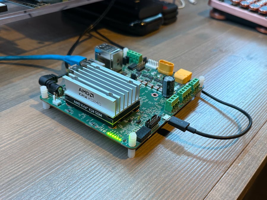
This year saw the release of AMD's next Kria SOM and development carrier board with the Kria K24 SOM and the KD240 Drives Starter Kit. I had the honor of working with AMD to create a DSP related project to demonstrate some of the capabilities of the Kria K24. Since that project, I've partnered with AMD again to do a series of getting started project guides for the Kria KD240 Drives Starter Kit. This project guide will walk through how to create a base hardware design on the KD240 with the hooks to the various peripherals on the carrier board as well as hooks for accelerated application design in Vitis/PetaLinux.
This project is done in Vivado 2023.2, and 2023.1 is the first version of the AMD FPGA tools that has support for the Kria K24 KD240 Drives Starter kit. So this tutorial is NOT backwards compatible with earlier versions of Vivado prior to 2023.1.
New Project in VivadoLaunch Vivado and select the option to create a new project. Start by specifying the desire project name and directory location.
Leave the default option selected for RTL Project as the Project Type. Check the option to not specify sources at this time (which refers to importing HDL source files during this part of creating the project). I'm also checking the option to make the project an extensible Vitis platform so that the hook will be there later on for accelerated application design in Vitis/PetaLinux.
For the Default Part, switch to the Boards tab and search for the KD240. Select the Kria KD240 Drives Starter Kit SOM.
Click on the Connections hyperlink under Kria KD240 Drives Starter Kit SOM to bring up the boards connections manager. While all of the Kria carrier boards show as an option, it is important to match Connector 1 and Connector 2 of the K24 SOM to the Drives Starter Kit carrier. Furthermore, be sure to match SOM240_1 to SOM240_1 and SOM40_2 to SOM40_2. This is critical as any mismatch will cause errors in signal routing between the Kria K24 SOM and the KD240 carrier board.
On the final screen of the New Project wizard, review and confirm all of the selections before clicking Finish to create the project.
Vivado will then launch into the new project:
The first step in any Zynq-7000 or Zynq UltraScale based project is to instantiate the respective Zynq Processing System IP core in the design such that the ARM-core processor with its various peripherals is accessible in the design.
The easiest way to do this is via the block design workflow in Vivado. So select the Create Block Design option from the Flow Navigator and specify the desired file name for it.
After specifying the desired file name for the block design and clicking OK, Vivado will automatically open the new blank block design.
Click the + button to open the IP catalog and type Zynq into the search bar. Click on the Zynq UltraScale+ MPSoC to add it to the block diagram.
The option to run block automation will then appear to apply the specific settings/configuration to the Zynq MPSoC IP for the Kria K24 on the KD240 carrier board.
Click the hyperlink in the green banner to Run Block Automation and ensure the option to Apply Board Preset is checked before clicking OK:
After digging through all of the settings and configured MIO peripherals, I found that I didn't need to manually add/configure anything like I had to for the Kria KR260 in 2022.x previously.
In other words, everything that is connected directly to the ARM-core processors in the Zynq MPSoC need no further configuration in the Vivado project, only peripherals connected to the programmable logic (PL) need to be configured as desired by the user.
Platform SetupI chose to preemptively make this hardware design an extensible Vitis platform so that I had the hooks for using it in accelerated application development as well as regular software application development without having to come back and rebuild it. The resources/peripherals specified in the Platform Setup tab within the block design are what will be visible with an accelerated application in Vitis.
While the following configuration is not a one-size-fits-all solution to any/all accelerated applications, I've found that it's a general enough design that it's a good base to start with until further specifics are needed. I accomplish this by giving the platform a dedicated 200MHz clock with its own Processor System Reset, a dedicated AXI Interrupt Controller, and an array of both regular and high-performance AXI interfaces.
First, reopen the Zynq MPSoC IP to configure the second PL clock. Under Clock Configuration, change pl_clk1 to 200MHz:
Then add an AXI Interrupt Controller to the block design and change its Interrupt Output Connection to Single:
Add a Processor System Reset and connect its slowest_sync_clk to pl_clk1.
Then run the connection automation for the AXI Interrupt Controller, leaving the default options selected:
The option to run connection automation will appear immediately again to connect the second M_AXI_HPM port of the Zynq MPSoC to the AXI Interconnect.
Finally, connect the irq output from the AXI Interrupt Controller to the pl_ps_irq input of the Zynq MPSoC:
With the peripherals configured in the block design, switch the the Platform Setup tab to enable them for accelerated development.
In the AXI Port section, under zynq_ultra_ps_e_0, enable all of the AXI interfaces except for S_AXI_LPD. I also specified a shorter SP tag for each (the name it will appear in Vitis as) to make life easier later when creating the accelerated application later.
I also enabled 8 regular AXI interfaces through the AXI interconnect in the deign as well (so with shorter SP tags).
Next in the Clock section, enable pl_clk1 and set it as the default clock to be used:
Enable the interrupt from the the AXI Interrupt Controller (irq) in the Interrupt section:
Finally, specify the desired platform name. It will default to <block design file name>_wrapper, but I personally like to rename them <device name>_base. So in this case, I named the platform kd240_base.
This naming convention is just a personal preference of mine as I feel like it helps keep everything in the workflow clear later on in Vitis and PetaLinux.
Add PeripheralsWith the Zynq MPSoC IP and Platform configured, the next thing to do in the design is to add the peripherals that are contained/routed through the PL.
There is a handy feature in Vivado under the Board tab within a block design that lists the hardware peripherals located on the target FPGA development board that must be connected via the PL (so this tab only appears in Vivado projects that target a development board, not just an FPGA part). Furthermore, when a peripheral is selected from this list, it will also show a culled list of IPs from the IP catalog that are compatible with it.
As a simple demonstration of this feature, I'll start with the two user LEDs that are on the KD240 board (UF1 and UF2). They are listed as USER_LED under the Board tab:
Right-click on the peripheral name and select the option Connect Board Component...
This will bring up the aforementioned list of culled IPs in the IP catalog that are compatible with the target peripheral. The option at the top of this list is what would be selected if the Auto Connect option is selected instead of Connect Board Component...
I just selected the top option of the first channel of an AXI GPIO:
This will add the AXI GPIO configured to match the peripheral (two bits of outputs to drive the LEDs) with the external port already connected. It still needs to be connected to the AXI interconnect however, so the option to run connection automation will appear for it.
Click the hyperlink in the green banner to the connection automation. Verify that the connection automation is going to connect the AXI GPIO IP to the pl_clk0 clock domain and not pl_clk1:
I personally like to validate the block design after adding each peripheral so errors/critical warnings are easier to track down. The user LEDs are the only peripheral I am adding from the Board tab in this manner at the moment.
I do have a critical warning that there is nothing driving the input interrupt on the AXI Interrupt Controller, however that can be safely ignored in this instance.
Motor Control LogicI only added the user LEDs from the Board tab because I wrote some custom HDL logic for driving a 3-phase brushless DC motor with encoder that I added to the block design as module IPs.
While my HDL is gears specifically towards the Kria KD240 Motor Accessory Pack based on the Anaheim Automation motor and encoder, how I am connecting everything in this design is the same as it would be for any other motor accessory packs. So if you develop custom IP by hand or in another software environment such as Simulink in Matlab, the following steps can be applied for connection with that IP.
While I plane to expand the communication interface of my motor control HDL, it currently just uses a single-bit input as a start/stop signal. To control this from the ARM-core processor of the Zynq MPSoC, I added another AXI GPIO IP from the main IP catalog (click the + button from the top of the Diagram window) configured with a 1-bit output:
I then ran the connection automation for this AXI GPIO, not selecting the option to automatically connect the GPIO output (I'm manually connecting it to my module in the next steps) and connecting the AXI interface to the AXI Interconnect on the pl_clk0 domain.
Since I wrote my own HDL, I added the HDL source files using the Add Sources option in the Flow Navigator:
My HDL includes driving the control word to the gate driver circuit for the 3-phase motor while reading back the output from the quadrature encoder for positioning. I will be covering the specifics of this and the HDL itself in a separate post as it is a bit of a complex topic. My only goal in this post is to demonstrate how to connect it since any other custom IP/HDL would need to be connected in a similar manner.
To add a custom HDL module to the block design, right-click anywhere in blank space in the Diagram window and select the option Add Module...
Then select the desired HDL module. In my case, that is the top level module of my HDL, motor_controller:
Ignore the option to run connection automation as it still wants to try to connect the output of the AXI GPIO.
Instead, I manually connected it to the start_stop input of my motor controller. I also connected the clock and reset signals of my motor controller to the same pl_clk0 domain that the AXI GPIO is.
There are four output signals that need to be made into external ports: the enable signal for the motor and the signals for the three gate drivers that ultimately drive the 3-phase brushless DC motor connected to the J32 Motor Connector on the KD240 carrier board.
This can be done by either right-clicking on each signal on the IP block and selecting Make External or highlighting the pin and using the ctrl+T keyboard shortcut:
Then repeat the process for the index and channel A/channel B inputs from the quadrature encoder coming from the J42 connector on the KD240 carrier board.
Overall, this is what my block design ended up looking like:
Once a block deign is completed, validated, and saved, there is the option to generate the block design. This is simply running synthesis and generating the output products for each IP within the block design, which would be done automatically when the option to run synthesis for the overall design is selected if it hadn't been done already. This is ultimately an option that can be used to breakup synthesis a bit so it doesn't take as long all in one pass.
Select Generate Block Design from the Flow Navigator. Leave the default options checked in the Generate Output Products window and click Generate.
The status of the synthesis run for each IP can be seen in the Design Runs tab in the bottom window.
Each completed synthesis run is marked by a green check mark. If modifications are then made to any of the IPs, an orange dot will appear on the green check mark indicating synthesis for that IP needs to be reran.
With the block design complete and each IP synthesized, the next step is to create an HDL wrapper file to instantiate the block design within the project and provide the hooks for the external ports to be connected to the FPGA's package pins via the constraints file.
Right-click on the block design file in the Sources window and select Create HDL Wrapper...
Vivado will then ask if it should automatically update the HDL wrapper file if subsequent edits are made to the block design, or just leave it up to the user to maintain. I personally always choose to let Vivado auto-update it.
In instances where I do need a custom top level HDL file, I just disable the auto-generated wrapper and re-enable it when I make edits to the block design so I always have it to copy+paste from. I've found it's an easy way to help cut down on self-inflicted errors.
ConstraintsFinally, the last part of the design is to tie the external port signals to specific FPGA package pins. The raw pinout constraints file for the K24 SOM in the Kria Wiki here:
That raw constraints file follows the naming convention of the high-density connectors that the Kria K24 SOM connects to the KD240 via, so I then used the schematic for the KD240 carrier board to determine which SOM pin went to my target signals such as the user LEDs, motor phase gate drivers, and single-ended quadrature encoder.
To create a new constraints file, select Add Sources from the Flow Navigator and select the option to Add or create constraints:
Create a new file with the desired file name.
I then simply copy+pasted the constraints from the raw constraints file and renamed them to match my top level signals and set them to the desired voltage values (the user LEDs are in the high-performance bank though so they have to be set at 1.8v):
With the design complete, run synthesis for the overall design (select Run Synthesis from the Flow Navigator):
Once synthesis has completed successfully, the option to run implementation will pop up:
And finally, generate a bitstream:
With the design completed and a bitstream generated, the final step in Vivado is to export the design in AMD's custom format (XSA) so that it can be imported into Vitis and PetaLinux to build a software design on.
Select File > Export > Export Platform...
This will bring up the export wizard:
Select either the option for the platform to be exported as just hardware or hardware plus hardware emulation:
Be sure to include the bitstream in the exported platform:
Then fill in the info fields as desired. I personally like to add a bit to the description for my future self.
The XSA file name will also default to <block design file name>_wrapper, and again I like to rename them <device name>_base to keep things clear later on in the software development flow in Vitis.
Finally the selected options can be reviewed before clicking Finish to export the platform into an XSA file.
From this point the next step is to import the XSA file into Vitis or PetaLinux to start software development, see my next project posts for those tutorials!


Comments
Please log in or sign up to comment.