(This project is being managed here: Project Repository )
The H bridge inverter is used to convert DC voltages to AC voltages. An h bridge is common in generating pure sine waveforms from DC square waveforms.
H-bridge consists of 4 switches which could be transistors or MOSFETs. In these switches, the voltage across the load changes polarity after each half cycle of the control signal which is being used to sequentially drive the switches. This creates the required AC waveform from a static DC supply.
Working:There are 2 control signals controlling the MOSFETs. When one is high the other is low. When output1 is high the LOW side of MOSFET connected with the signal is turned ON and the BJT transistor is also turned on which pulls the gate pin of the high side MOSFET to the ground thus turning it OFF. Whenever output1 becomes low and thus turns OFF the low side MOSFET, the high side MOSFET is turned on by the voltage that was across the capacitor. This is how the other will also work the same. The H bridge works by turning ON each pair of diagonal MOSFETS in every half cycle.
Schematic:There are two schematics files; one is for square wave generation and the other one is for H-bridge operation. I have designed a schematic diagram in Altium Designer. I have created an empty project online on Inventhub and uploaded my schematic file there. Making project online is helpful for the users who want to implement my design. They can visually view and download it from the Inventhub easily and can directly implement the design without any error.
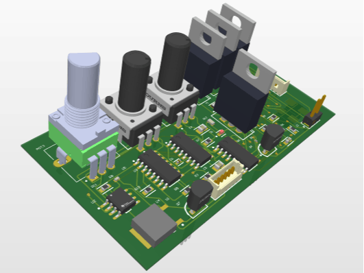
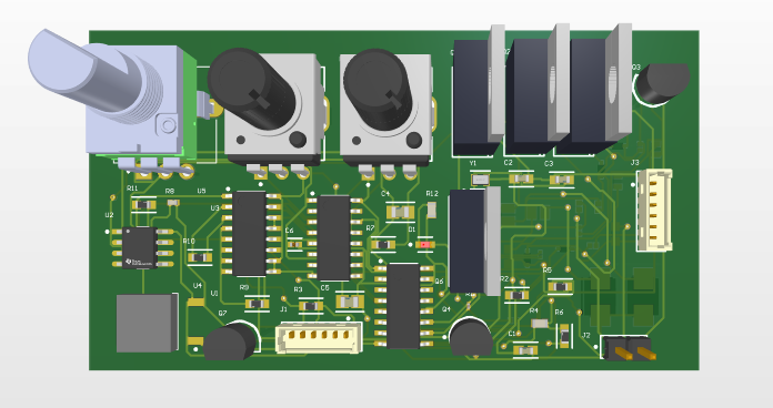
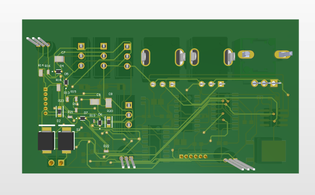
For the fabrication, I have converted my schematic file to the PCB file. Here I can view my board in 3D, check for errors, and edit the shape of the board. I have uploaded my PCB file on Inventhub. Instead of visiting the manufacturer, I can send him the PCB file, he can easily download it and can fabricate my board. This is also useful for the users who want to design my board, they can view and download it from the Inventhub.
Design for Manufacturing:To get my whole project in one place, I have created a release file of my project after uploading all my design files on Inventhub. This file contains my schematic, PCB, library, and all history files in a ZIP file format. For fabrication, the manufacturer, instead of viewing and downloading each file one by one, just needs to download this release file and he can easily fabricate my PCB without making any errors.
I have created a BOM file in Altium then I uploaded it in CSV format on Inventhub where I can calculate the total cost of my design by selecting the ‘supply chain’ option. I can view the components and can read their datasheets also. I can select my distributor for the components depending on the price and availability of the components. The total cost of this project is $26.478. My component provider can easily download this BOM file and can deliver my components as per my design requirements.


Comments
Please log in or sign up to comment.