


Hardware components | ||||||
 |
| × | 1 | |||
 |
| × | 1 | |||
| × | 1 | ||||
 |
| × | 1 | |||
Software apps and online services | ||||||
 |
| |||||
 |
| |||||
 |
| |||||
| ||||||
| ||||||
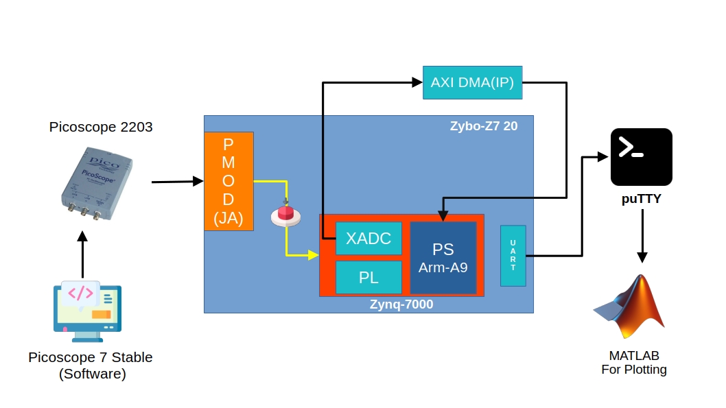
The world primarily operates with analog signals; however, computers and embedded systems are most efficient when processing signals in the digital domain. To enable such processing, analog signals must first be converted into digital format, which highlights the importance of Analog-to-Digital Converters (ADCs). In this project, I will leverage the built-in ADC, also known as XADC, on the AMD Xilinx Zynq-7000 SoC. The system will read data from an external analog input (data acquisition will commence only upon pressing a button) and digitize it using the XADC. The digitized data will then be transferred to the Processing System (PS) RAM via AXI Direct Memory Access (DMA) and subsequently plotted in MATLAB. The system-level diagram is illustrated in Figure 1.
For this project, I am utilizing the Digilent Zybo-Z7 20 board. To begin, let's take a brief look at the XADC integrated into the Zynq-7000 SoC.
XADC FunctionsThe XADC on the Zynq-7000 chip performs two main functions:
- It reads the zynq temperature from the temperature sensor and different zynw power rails.
- Secondly, it converts analog signals to digital from external channels.
**Note: In this tutorial, we will mainly focus on reading data from an external analog port.
The XADC can be utilized by instantiating the XADC Wizard IP in your hardware design. The configuration and operation of the XADC depend on your application's requirements and the method of control chosen:
XADC Configuration MethodsStatic Configuration via XADC Wizard
- All settings can be predefined during IP configuration in the Vivado environment.
- Suitable if no runtime changes to the XADC setup are required.
Dynamic Configuration via xsysmon.h
- Applicable when the AXI4Lite interface is enabled for the XADC Wizard IP.
- Allows real-time modifications to the configuration, such as:
- Switching between input channels.
- Adjusting other runtime parameters.
This tutorial adopts this approach for better flexibility.
Control via FPGA Logic
- Use the Dynamic Reconfiguration Port (DRP) interface to control XADC directly from FPGA logic.
- DRP offers low-level control but is outside the scope of this tutorial.
The XADC supports multiple operating modes (refer to UG480 for details). For simplicity, this tutorial focuses on:
Single Channel Mode
- Configures the XADC to sample a single input channel.
Continuous Sampling Mode
- The XADC continuously acquires and converts analog signals into a stream of digital data.
- This data stream will be processed via DMA for efficient handling.
By combining continuous sampling and single channel mode, the XADC setup ensures a consistent stream of data for applications like real-time signal monitoring and processing.
XADC ChannelsThe XADC on the Zynq-7000 can read a single external input channel at a time, with the capability to switch between multiple channels. It includes:
- DedicatedAnalog Input Channel: A primary analog input channel named VP/VN.
- Auxiliary Channels: Sixteen additional differential input channels, labeled VAUX [0..15].
Each auxiliary channel features two differential input signals:
- Positive Input: Referred to as VP or VAUXP.
- Negative Input: Referred to as VN or VAUXN.
***Note: However, in this tutorial we will be using auxilary channels because the Zybo-Z7 20 board doesnot have any external PMOD connected to the the dedicated input channel
XADC Resolution OverviewThe Zynq-7000 XADC features a 12-bit ADC capable of measuring voltages from 0 to 3.3 V with a resolution of approximately 0.8 millivolts.
However, additional details enhance its precision and functionality:
16-bit Conversion Results:
- The XADC status registers and the
XSysMon_GetAdcData()function store conversion results in 16-bit format. - The lower 4 least significant bits (LSBs) can be ignored for standard 12-bit precision.
Averaging for Enhanced Precision:
- The XADC can be configured to average consecutive 16, 64, or 256 samples.
- In this mode, the additional 4 LSBs are used to represent the averaged value, improving precision beyond the standard resolution.
The XADC is driven by two key clocks:
- DCLK: Drives the XADC Wizard and is linked to the
s_axi_aclkof the AXI interface. - ADCCLK: Powers the ADC circuitry and is derived from DCLK using a configurable divider (2–255). This ratio can be dynamically configured with
XSysMon_SetAdcClkDivisor().
The XADC wizard
Continuous Sampling Mode:
- 26 ADCCLK cycles are required for acquiring and converting a signal.
- This period can extend to 32 cycles by enabling the
IncreaseAcqCyclesparameter viaXSysMon_SetSingleChParams(). - The extra cycles increase the "settling period, " also known as "Acquisition Time, " for better precision with certain input signals.
Settling Period Terminology:
Xilinx documentation uses varying terms:
- "Settling Period" in UG480.
- "Acquisition Time" in the XADC Wizard UI and code comments.
- UG480 clarifies that this period (default: 4 ADCCLK cycles, extendable to 10) is part of the overall acquisition time
Maximum Sampling Rate:
Achieved at 1 Msps with:
- DCLK = 104 MHz
- Divider Ratio = 4
- Resulting in ADCCLK = 26 MHz.
Adjusting Sampling Rates:
- Set DCLK frequency and divider ratio to achieve:
- Desired ADCCLK Frequency=26×Desired Sampling Rate
For example:
To achieve 100 kSPs:
- DCLK = 101.4 MHz
- Divider = 39
Guaranteed Analog Bandwidth:
- Auxiliary Channels: Limited to 250 kHz for full resolution, even if sampled at 1 Msps.
- VP/VN Dedicated Input: Assumed to support at least 500 kHz bandwidth, corresponding to the Nyquist frequency for 1 Msps.
Practical Considerations:
- Sampling at 1 Msps may not always be ideal due to the characteristics of the input signal and front-end circuitry. Input signals with higher frequency content require careful consideration to ensure accuracy
The Zybo Z7-20 board offers six PMOD connectors for interfacing with various peripherals. Of these, PMOD JA is specifically connected to the XADC.
The pin configurations are depicted in the Figure 3 below:
It is important to note that on the Zybo-Z7 board, only four XADC auxiliary channels are connected to PMOD JA. Therefore, to provide an analog signal to the XADC, the input must be connected to one of these pins. According to the Zybo-Z7 reference manual:
The Dual Analog/Digital Pmod on the Zybo Z7 differs from the rest in the routing of its traces. The eight data signals are grouped into four pairs, with the pairs routed closely coupled for better analog noise immunity. Pins 1 and 7, pins 2 and 8, pins 3 and 9, and pins 4 and 10 are paired up. Furthermore, each pair has a partially loaded anti-alias filter laid out on the PCB. The filter does not have capacitors C101-C104 loaded. In designs where such filters are desired, the capacitors can be manually loaded by the user.
For additional context, the Pmod ports on the Zybo-Z7 are 2×6, right-angle, 100-mil-spaced female connectors designed to interface with standard 2×6 pin headers. Each 12-pin Pmod port provides two 3.3V VCC signals (pins 6 and 12), two ground signals (pins 5 and 11), and eight logic signals, as illustrated in the Figure 4 below:
To begin, create a new project in AMD Vivado and name it XADC_EXAMPLE_PROJECT. Save the project in your preferred directory.
Next, we need to specify the type of project. I will select the RTL Project option. There are two sub-options to choose from. I will check the option Do not specify sources at this time to skip the "Add Sources" window and proceed directly to board selection. The sources can be added later in the project. The second option will remain unchecked, but it can be modified at a later stage in the project.
Next, we need to add either a part or a board to the project. I prefer adding the board, as Vivado automatically configures certain settings for us once the board is specified. This includes setting up constraints for the available IPs and resources. Additionally, we can directly add peripherals to the design without needing to specify them in the constraint file. Since I am using a Digilent board, which is not manufactured by AMD Vivado but rather a third-party vendor, I will need to add the board files to Vivado. The guide to adding Digilent board files can be found here. I will select my Zybo-Z7 20 board on the boards tab.
At the last tab, you will see the New Project Summary. Click finish, and we are ready to begin our design.
In order for our design to talk with the external buttons and PMODs, we need to set up a constraint file. The digilent boards constraint files can be downloaded from this link. In the master directory, locate the file named Zybo-Z7-Master.xdc and download it. Then, from the Flow Navigator on the right, under the Project Manager heading, select Add Sources.
A new window will appear from there Select "Add or create constraints."
Click on Add Files and locate the Zybo-Z7-Master.xdc file and open it. Click Finish
Under the sources tab and in the constraints directory, you will be able to locate this file.
Double-click the Zybo-Z7-Master.xdc file to open it in a text editor within the Vivado environment. For this design, we will be using two external interfaces: one for the button and the other for the PMODs. Specifically, the design includes a button at K18 and an auxiliary channel VAUX14 at AD14 (N15 & N16). Figure 11 illustrates the modifications made to the constraint file.
From the Flow Navigator on the left under IP Integrator heading, click "Create Block Design."
This will open a new window prompting you to enter the design name. You can leave the remaining settings at their default values. Click OK, and this will open the diagram window.
***Note: I highly recommend avoiding the use of folders or file names with spaces when saving any files related to AMD Vitis, Vivado, or Vitis HLS. Instead, use camel case or another programming standard naming convention to ensure compatibility and prevent potential issues.
There are several ways to add IPs to the design. You can either right-click on the screen and select Add IP or press CTRL+I.
We will begin by adding the Zynq Processor to the design. Press CTRL+I, type "Zynq, " and select ZYNQ7 Processing System. Once added, the DesignerAssistance tab will appear at the top of the window. Click Run Block Automation on this tab.
This will open a window with recommendations based on the specified board, suggesting that the DDR and Fixed I/O ports on the PS be connected to external interfaces. Click OK to proceed. The process may take some time as Vivado automatically establishes these connections.
We need to configure the PS to proceed further. Double-click the Zynq PS IP to reconfigure it. Enable the S AXI HP0 slave interface. This high-performance port will be used by AXI DMA to write data to RAM.
Next, enable the 28 GPIO pins of the PS. These pins will be used to receive input from the button to initiate data reception and to control the number of data transfers.
The Zynq-7000 chip features 64 EMIO pins, with the first 32 pins (pins 54-85) located in Bank 2. Figure 20 illustrates the pin allocation and how these pins will be utilized in the design.
To begin, let's connect the buttons. Right-click on the block diagram screen and select Add Port. In the constraint file, we have defined the button as btn, so name the port btn and configure the settings as shown in the Figure 21
Since we have configured 28 EMIO pins and only one bit is required for the button, I will concatenate a 27-bit constant to the btn. To do this, add a Constant IP and set the configurations as shown in the Figure 22:
Add a concat IP and customize it as shown in Figure 23:
Connect the block diagrams as shown in Figure 24
As discussed in the Sampling Rate section, we need a DCLK to drive the XADC. The default output clock from the PS is 50 MHz, but we require a DCLK of 104 MHz. To achieve this, I will use the Clocking Wizard. Add the Clocking Wizard IP and customize it according to the settings shown in the Figure 25.
Set the output clock to 104 MHz. In the XADC wizard, by setting the divider ratio to 4, we can achieve a 26 MHz clock for the ADDCLK of the XADC. In the Clocking Wizard, set the reset type to Active Low to ensure it aligns with the rest of the processor resets.
Now, add a Clocking Wizard IP to your design and re-customize it. Most of the control for the XADC will be handled using xsysmon.h in the Vitis environment, so only the bare minimum re-customization of this IP is required. Adjust the configuration according to the settings shown in the Figure 27:
In the single channel mode tab enable the VAUXP14 VAUXN14 channel because that is what we will be using for our digitization.
Run the connection automation to establish all the necessary connections as shown in the figure below. Vivado will automatically handle many tasks, such as adding the processor reset block and AXI interconnects.
At this point, the XADC is configured, and now we need to add the logic to transfer the data to the RAM of the Zynq PS. This task will be accomplished using AXI DMA. However, it is important to note that AXI DMA requires a tlast signal to indicate that the last bit of data is being transmitted. Since the XADC in our design does not have this functionality, we will need to build a custom IP to generate this signal.
Additionally, there is a limit to the amount of data that AXI DMA can transfer in a single cycle, which is 26 bits. We will implement this limitation using our custom IP, which will receive a 25-bit count value along with a start signal from the PS.
Let’s proceed with creating our custom IP. From the top bar, under the Tools menu, click Create and Package New IP. This will open a new window; click Next. In the next step, check the box labeled Create a New AXI4 Peripheral and then click Next.
Next name your IP and set its location. Click Next.
In the Add Interfaces window, add two AXI stream interfaces: one in slave mode and the other in master mode. Keep the rest of the configurations in their default settings. Once done, click Next.
On next tab under Next steps click edit IP and enter Finish.
You will have a new window open. Under design sources delete all the files except the top module. Open the top module for editing.
Delete all the existing Verilog code in the top module and replace it with the code provided below. This code has been sourced from Viktor Nikolov's tutorial on GitHub.
/*
This Verilog module is part of the XADC tutorial. It controls when the data from
the slave AXI-Stream interface starts to be sent to the master AXI-Stream interface.
It also controls how many data transfers are made and asserts the TLAST signal
on the last transfer.

Details are explained on GitHub: https://github.com/viktor-nikolov/Zynq-XADC-DMA-lwIP

BSD 2-Clause License:

Copyright (c) 2024 Viktor Nikolov

Redistribution and use in source and binary forms, with or without
modification, are permitted provided that the following conditions are met:
1. Redistributions of source code must retain the above copyright notice, this
   list of conditions and the following disclaimer.
2. Redistributions in binary form must reproduce the above copyright notice,
   this list of conditions and the following disclaimer in the documentation
   and/or other materials provided with the distribution.
THIS SOFTWARE IS PROVIDED BY THE COPYRIGHT HOLDERS AND CONTRIBUTORS "AS IS"
AND ANY EXPRESS OR IMPLIED WARRANTIES, INCLUDING, BUT NOT LIMITED TO, THE
IMPLIED WARRANTIES OF MERCHANTABILITY AND FITNESS FOR A PARTICULAR PURPOSE ARE
DISCLAIMED. IN NO EVENT SHALL THE COPYRIGHT HOLDER OR CONTRIBUTORS BE LIABLE
FOR ANY DIRECT, INDIRECT, INCIDENTAL, SPECIAL, EXEMPLARY, OR CONSEQUENTIAL
DAMAGES (INCLUDING, BUT NOT LIMITED TO, PROCUREMENT OF SUBSTITUTE GOODS OR
SERVICES; LOSS OF USE, DATA, OR PROFITS; OR BUSINESS INTERRUPTION) HOWEVER
CAUSED AND ON ANY THEORY OF LIABILITY, WHETHER IN CONTRACT, STRICT LIABILITY,
OR TORT (INCLUDING NEGLIGENCE OR OTHERWISE) ARISING IN ANY WAY OUT OF THE USE
OF THIS SOFTWARE, EVEN IF ADVISED OF THE POSSIBILITY OF SUCH DAMAGE.
*/
`timescale 1ns / 1ps

module stream_tlaster(
    input clk,          // AXI-Stream clock
    input start,        // When asserted, starts sending data to the master AXI-Stream
    input [24:0] count, // Number of data records to be sent before tlast is asserted

    //Master AXI-Stream signals
    output reg [15:0] m_axis_tdata,
    output reg m_axis_tvalid,
    output reg m_axis_tlast,
    input m_axis_tready,

    //Slave AXI-Stream signals
    input [15:0] s_axis_tdata,
    input s_axis_tvalid,
    output reg s_axis_tready
);

    // State definitions
    localparam IDLE = 0,
               RUNNING = 1,
               WAIT_FOR_TREADY = 2;

    // State and internal signals
    reg [1:0] state = IDLE;
    reg [24:0] valid_count;
    reg s_axis_tvalid_prev;

    // Next state logic and outputs
    always @(posedge clk) begin
        case (state)
            IDLE: begin
                // Reset everything
                valid_count <= 0;
                s_axis_tvalid_prev <= 0;
                m_axis_tlast <= 0;
                m_axis_tvalid <= 0;
                // We keep tready asserted in IDLE to keep the source producing the data
                s_axis_tready <= 1;

                // Transition to RUNNING when start is asserted
                if (start)
                    state <= RUNNING;
            end
            RUNNING: begin
                // Pass through data, valid and ready signal
                m_axis_tdata <= s_axis_tdata;
                m_axis_tvalid <= s_axis_tvalid;
                s_axis_tready <= m_axis_tready;

                // Check for transition from 0 to 1 in s_axis_tvalid
                if (!s_axis_tvalid_prev && s_axis_tvalid) begin
                    valid_count <= valid_count + 1;
                    // Check if the transition count reaches 'count'
                    if (valid_count == count-1) begin
                        m_axis_tlast <= 1;
                        state <= WAIT_FOR_TREADY;
                    end else begin
                        m_axis_tlast <= 0;
                    end
                end else begin
                    m_axis_tlast <= 0;
                end

                // Update the previous valid signal state
                s_axis_tvalid_prev <= s_axis_tvalid;
            end
            WAIT_FOR_TREADY: begin
                /* To comply with AXI-Stream specification, we can deassert
                   tvalid and tlast only if m_axis_tready is high. */
                if( m_axis_tready ) begin
                    m_axis_tlast <= 0;
                    m_axis_tvalid <= 0;
                    state <= IDLE;
                end
            end
        endcase
    end

endmodule
Click on the Package IP tab. Under Packaging Steps, go to File Groups. At the top, you will see a message that says "Merge changes from File Groups Wizard." Click on it.
Repeat the same steps for the Customization Parameters and Ports and Interfaces sections. Once you have completed these steps, navigate to Review and Package. At the bottom, click Re-package IP. Your IP is now ready to be used in your project.
Go to your Vivado project and search for the new IP you created. Add it to your design. Next, add the AXI DMA IP and configure it according to Figure 38.
Your hardware design is now ready to be converted into an HDL wrapper and exported to the Vitis IDE. The final block diagram should resemble Figure 39.
Under design sources right click your block design and click create HDL wrapper and select option "Let Vivado manage wrapper and auto-update".
Once your design is ready, under the Flow Navigator bar, click Generate Bitstream. This will perform all the necessary steps, including Synthesis and Implementation. Finally, from the main menu, click File → Export → Export Hardware. In the output window that appears, select the option "Include Bitstream", choose the location, and click Finish.
**Note: It is recommended to keep your exported hardware file in the same directory as your vivado project.
Writing Software In VitisFor this project, I am using the Vitis Classic IDE instead of the Vitis Unified Platform, primarily because I am more familiar with the classic version. 😌 Open your Vitis IDE and create a new Vitis application project.
Under "Create a new platform from hardware (XSA)" specify the XSA file you exported from hardware.
Give your application a name and vivado will pick up the system project name itself. Select the processor core by defalult it is ps7_cortexa9_0.
Leave everything on the next tab as it is. keep the operating system as standalone.
From the available templates, select the Hello World template, which is a simple program that helps you get started with writing and running code on your embedded platform. Click Finish to proceed.
Once the project is created, locate the helloworld.c file in the src folder of your project and open it in the editor. Replace the existing code with the following updated code. The code has been commented with explanations at each step to help you understand its functionality and how it interacts with the hardware.
// Including necessary header files for Xilinx hardware and software libraries
#include "xsysmon.h"    // Header for XADC system monitor functions
#include "xparameters.h" // System parameters definitions
#include "xil_types.h"   // Basic data type definitions for Xilinx systems
#include "xgpiops.h"     // Header for GPIO functions
#include "xaxidma.h"     // Header for AXI DMA controller functions
#include "platform.h"    // Platform-specific definitions
#include "xil_printf.h"  // Functions for formatted output
#include <stdio.h>       // Standard I/O functions
#include <stdint.h>      // Standard integer type definitions
#include <string.h>      // String manipulation functions

// Define the number of samples to be transferred in one DMA operation
#define SAMPLE_COUNT 1000

// Define the GPIO pin for button BTN0
#define BTN0_PIN 81 // This is GPIO pin 0 in Bank 2 (EMIO pins)

// Ensure the sample count does not exceed the AXI DMA maximum transfer size
#if SAMPLE_COUNT > 0x01FFFFFF
    #error "SAMPLECOUNT exceeds the maximum limit"
#endif

// Define whether the XADC should average samples or not
#define AVERAGING_MODE XSM_AVG_0_SAMPLES

// Buffer to hold data for DMA transfers, aligned to 4 bytes for efficiency
static u16 DataBuffer[SAMPLE_COUNT + 8] __attribute__((aligned(4)));

// Instances for peripherals
static XGpioPs GpioInstance;      // GPIO instance for controlling inputs and outputs
static XSysMon XADCInstance;     // XADC system monitor instance
static XAxiDma AxiDmaInstance;   // AXI DMA instance for data transfer

// Enum for selecting XADC input channels
typedef enum eXADCInput {
    VAUX14, // Auxiliary analog input channel 14
    VPVN    // Dedicated bipolar channel VP/VN
} eXADCInput;

// Variable to hold the currently activated XADC input
eXADCInput ActivateXADCInput;

// Pointer to a function for converting raw XADC data to voltage
static float (*Xadc_RawToVoltageFunc)(u16 RawData);

// Define system clock frequency in Hz (used for delay calculations)
#define SYSTEM_CLOCK_FREQUENCY_HZ 100000000 // 100 MHz

// Function to create a delay in milliseconds using a busy-wait loop
void delay_ms(uint32_t milliseconds) {
    // Calculate delay in clock cycles
    uint32_t delay_cycles = SYSTEM_CLOCK_FREQUENCY_HZ / 1000 * milliseconds;
    // Busy-wait loop
    for (uint32_t i = 0; i < delay_cycles; i++) {
        // Do nothing, just wait for the cycles to pass
    }
}

// Initialize GPIO pins for use
static int GPIOInitalize() {
    XGpioPs_Config *GpioConfig; // Configuration pointer
    int Status;

    // Lookup configuration for the GPIO controller
    GpioConfig = XGpioPs_LookupConfig(XPAR_PS7_GPIO_0_DEVICE_ID);
    if (GpioConfig == NULL) {
        xil_printf("XGpioPs_LookupConfig failed! Terminating\n");
        return XST_FAILURE;
    }

    // Initialize GPIO controller with the configuration
    Status = XGpioPs_CfgInitialize(&GpioInstance, GpioConfig, GpioConfig->BaseAddr);
    if (Status != XST_SUCCESS) {
        xil_printf("XGpioPs_CfgInitialize failed! Terminating\n");
        return XST_FAILURE;
    }

    // Set the direction of GPIO Bank 2 pins (pins 54–80) as outputs
    XGpioPs_SetDirection(&GpioInstance, 2 /*Bank 2*/, 0x03FFFFFF);

    // Write initial values: sample count and stop/start signal
    XGpioPs_Write(&GpioInstance, 2 /*Bank 2*/, SAMPLE_COUNT << 1);

    // Enable output on the configured pins
    XGpioPs_SetOutputEnable(&GpioInstance, 2 /*Bank 2*/, 0x03FFFFFF);

    return XST_SUCCESS;
}

// Conversion function for XADC raw data to voltage for channel VAUX14
static float Xadc_RawToVoltageAUX14(u16 RAWDATA) {
    const float Scale = 3.32; // Scale factor for conversion to voltage

#if AVERAGING_MODE == XSM_AVG_0_SAMPLES
    // If averaging is disabled, use only the top 12 bits
    return Scale * ((float)(RAWDATA >> 4) / (float)(0xFFF));
#else
    // If averaging is enabled, use all 16 bits
    return Scale * ((float)RAWDATA / (float)(0xFFFF));
#endif
}

// Conversion function for XADC raw data to voltage for bipolar VP/VN channel
static float Xadc_RawToVoltageVPVN(u16 RawData) {
#if AVERAGING_MODE == XSM_AVG_0_SAMPLES
    // Handle special cases for the lowest negative value
    if ((RawData >> 4) == 0x800)
        return -0.5;

    float sign;

    // Determine the sign and convert raw data to absolute value if negative
    if (RawData & 0x8000) {
        sign = -1.0;
        RawData = ~RawData + 1;
    } else {
        sign = 1.0;
    }

    // Scale the raw data to voltage
    return sign * ((float)(RawData >> 4) * (1.0 / 4096.0));
#else
    if (RawData == 0x8000)
        return -0.5;

    float sign;

    if (RawData & 0x8000) {
        sign = -1.0;
        RawData = ~RawData + 1;
    } else {
        sign = 1.0;
    }

    return sign * ((float)RawData * (1.0 / 65535.0));
#endif
}
// Function to convert 12-bit unsigned value to signed 16-bit integer
static int16_t Convert12BitToSigned16Bit(u16 num)
{
    // Check if the number is negative by checking the 12th bit (sign bit)
    if (num & 0x800) {
        // If negative, sign-extend to 16 bits by setting the upper 4 bits
        num |= 0xF000;
    }
    // Return the signed 16-bit result
    return (int16_t)num;
} // Convert12BitToSigned16Bit

// Function to convert raw value of the XADC Gain Calibration Coefficient to a percentage of gain correction
static float ConvertRawGainCoefToPercents(u16 num)
{
    // Bottom 6 bits contain the number of tenths of a percent
    float res = (num & 0x3F) * 0.1;

    // The 7th bit is the sign bit, value 0 means negative coefficient
    if ((num & 0x40) == 0) {
        res *= -1; // If the 7th bit is 0, the coefficient is negative
    }

    // Return the calculated percentage value
    return res;
} // ConvertRawGainCoefToPercents

// Initialize the XADC (Xilinx Analog-to-Digital Converter)
static int XADCInitialize()
{
    XSysMon_Config *ConfigPtr;
    XStatus Status;

    // Look up the XADC configuration using the device ID
    ConfigPtr = XSysMon_LookupConfig(XPAR_XADC_WIZ_0_DEVICE_ID);
    if (ConfigPtr == NULL) {
        printf("XSysMon_LookupConfig failed! Terminating.\n");
        return XST_FAILURE;
    }

    // Initialize the XADC system monitor with the configuration
    Status = XSysMon_CfgInitialize(&XADCInstance, ConfigPtr, ConfigPtr->BaseAddress);
    if (Status != XST_SUCCESS) {
        printf("XSysMon_CfgInitialize failed! Terminating.\n");
        return XST_FAILURE;
    }

    // Print calibration coefficients (Offset and Gain Error)
    u16 ADCOffsetCoeff = XSysMon_GetCalibCoefficient(&XADCInstance, XSM_CALIB_ADC_OFFSET_COEFF);
    printf("calib coefficient ADC offset: %04X (%d bits)\n",
           ADCOffsetCoeff,
           Convert12BitToSigned16Bit(ADCOffsetCoeff >> 4));

    u16 GainCoeff = XSysMon_GetCalibCoefficient(&XADCInstance, XSM_CALIB_GAIN_ERROR_COEFF);
    printf("calib coefficient gain error: %04X (%.1f%%)\n",
           GainCoeff,
           ConvertRawGainCoefToPercents(GainCoeff));

    // Disable interrupts
    XSysMon_IntrGlobalDisable(&XADCInstance);

    // Set XADC to use Single Channel mode (not sequencer mode)
    XSysMon_SetSequencerMode(&XADCInstance, XSM_SEQ_MODE_SINGCHAN);

    // Disable alarms
    XSysMon_SetAlarmEnables(&XADCInstance, 0);

    // Disable averaging for calibration coefficient calculations
    u32 RegValue = XSysMon_ReadReg(XADCInstance.Config.BaseAddress, XSM_CFR0_OFFSET);
    RegValue |= XSM_CFR0_CAL_AVG_MASK; // Set bit to disable averaging
    XSysMon_WriteReg(XADCInstance.Config.BaseAddress, XSM_CFR0_OFFSET, RegValue);

    // Set averaging mode for measurements (value of AVERAGING_MODE macro is defined elsewhere)
    XSysMon_SetAvg(&XADCInstance, AVERAGING_MODE);

    // Enable offset and gain calibration based on the external/internal voltage reference
    u16 CalibrationEnables;
    if (GainCoeff != 0x007F) {
        // External voltage reference used
        CalibrationEnables = XSM_CFR1_CAL_ADC_GAIN_OFFSET_MASK | XSM_CFR1_CAL_PS_GAIN_OFFSET_MASK;
    } else {
        // Internal voltage reference used
        CalibrationEnables = XSM_CFR1_CAL_ADC_OFFSET_MASK | XSM_CFR1_CAL_PS_OFFSET_MASK;
    }

    // Apply the calibration enables based on reference selection
    XSysMon_SetCalibEnables(&XADCInstance, CalibrationEnables);

    return XST_SUCCESS;
} // XADCInitialize

// Activate the XADC input (either VAUX14 or VP/VN)
static int ActivateXADCInput1()
{
    XStatus Status;

    // Set ADC clock frequency to 1/4 of the XADC input clock for 1 Msps sampling rate
    XSysMon_SetAdcClkDivisor(&XADCInstance, 4);

    // If VAUX14 is selected as input
    if (ActivateXADCInput == VAUX14) {
        // Set parameters for VAUX14 input channel (single-ended unipolar mode)
        Status = XSysMon_SetSingleChParams(&XADCInstance,
                                           XSM_CH_AUX_MIN + 14, // Channel index for VAUX14
                                           0,                  // No additional acquisition cycles
                                           0,                  // Continuous sampling mode
                                           0);                 // Unipolar mode
        if (Status != XST_SUCCESS) {
            printf("XSysMon_SetSingleChParams for VAUX[1] failed! Terminating.\n");
            return XST_FAILURE;
        }

        // Assign the function pointer to convert raw samples from VAUX14 to voltage
        Xadc_RawToVoltageFunc = Xadc_RawToVoltageAUX14;
        printf("VAUX[1] is activated as the input.\n");
    }
    // If VP/VN is selected as input
    else if (ActivateXADCInput == VPVN) {
        // Set parameters for VP/VN input channel (differential bipolar mode)
        Status = XSysMon_SetSingleChParams(&XADCInstance,
                                           XSM_CH_VPVN,      // Channel for VP/VN
                                           0,                // No additional acquisition cycles
                                           0,                // Continuous sampling mode
                                           1);               // Differential mode (bipolar)
        if (Status != XST_SUCCESS) {
            printf("XSysMon_SetSingleChParams for VP/VN failed! Terminating.\n");
            return XST_FAILURE;
        }

        // Assign the function pointer to convert raw samples from VP/VN to voltage
        Xadc_RawToVoltageFunc = Xadc_RawToVoltageVPVN;
        printf("VPVN is activated as the input.\n");
    } else {
        printf("Called ActivateXADCInput() for an unknown input!\n");
        return XST_FAILURE;
    }

    return XST_SUCCESS;
} // ActivateXADCInput

// Initialize AXI DMA (Direct Memory Access)
static int DMAInitialize()
{
    XAxiDma_Config *cfgptr;
    XStatus Status;

    // Lookup the DMA configuration
    cfgptr = XAxiDma_LookupConfig(XPAR_AXI_DMA_0_DEVICE_ID);
    if (cfgptr == NULL) {
        printf("XAxiDma_LookupConfig failed! Terminating.\n");
        return XST_FAILURE;
    }

    // Initialize DMA with the configuration
    Status = XAxiDma_CfgInitialize(&AxiDmaInstance, cfgptr);
    if (Status != XST_SUCCESS) {
        printf("XAxiDma_CfgInitialize failed! Terminating.\n");
        return XST_FAILURE;
    }

    // Disable interrupts for DMA
    XAxiDma_IntrDisable(&AxiDmaInstance, XAXIDMA_IRQ_ALL_MASK, XAXIDMA_DEVICE_TO_DMA);
    XAxiDma_IntrDisable(&AxiDmaInstance, XAXIDMA_IRQ_ALL_MASK, XAXIDMA_DMA_TO_DEVICE);

    return 0;
} // DMAInitialize

// Perform a DMA transfer from XADC into RAM
static int ReceiveData()
{
    // Flush any data held in CPU cache to RAM for DataBuffer
    Xil_DCacheFlushRange((UINTPTR)DataBuffer, sizeof(DataBuffer));

    // Start the DMA transfer from XADC to RAM
    XStatus Status;
    Status = XAxiDma_SimpleTransfer(&AxiDmaInstance, (UINTPTR)DataBuffer, SAMPLE_COUNT * sizeof(u16), XAXIDMA_DEVICE_TO_DMA);
    if (Status != XST_SUCCESS) {
        printf("XAxiDma_SimpleTransfer failed! Terminating.\n");
        return XST_FAILURE;
    }

    // Trigger the start signal to begin data generation
    XGpioPs_WritePin(&GpioInstance, 54, 1 /*high*/);
    XGpioPs_WritePin(&GpioInstance, 54, 0 /*low*/);  // Reset the signal

    // Wait for the DMA transfer to complete
    while (XAxiDma_Busy(&AxiDmaInstance, XAXIDMA_DEVICE_TO_DMA)) {
        delay_ms(1); // Wait for 1 ms
    }

    // Invalidate the CPU cache to ensure the CPU fetches data from RAM
    Xil_DCacheInvalidateRange((UINTPTR)DataBuffer, sizeof(DataBuffer));

    return 0;
} // ReceiveData
// Additional functions omitted here for brevity but should follow the same detailed commenting structure
int XADC_function(void) {
    // Print the start message for XADC function
    xil_printf("***** XADC FUNCTION STARTED *****\n");
    xil_printf("Samples per DMA transfer: %d\n", SAMPLE_COUNT);

    // Initialize the GPIO, XADC, and DMA subsystems
    if (GPIOInitalize() == XST_FAILURE) {
        xil_printf("GPIO initialization failed!\n");
    }
    if (XADCInitialize() == XST_FAILURE) {
        xil_printf("XADC initialization failed!\n");
    }
    if (DMAInitialize() == XST_FAILURE) {
        xil_printf("DMA initialization failed!\n");
    }

    // Set the parameters for the XADC channel (VAUX14 in this case)
    if (XSysMon_SetSingleChParams(&XADCInstance, XSM_CH_AUX_MIN + 14, 0, 0, 0) != XST_SUCCESS) {
        printf("Failed to set VAUX14 as input!\n");
        return -1;  // Return error if setting the channel fails
    }

    // Set the channel to VAUX14 for activation
    ActivateXADCInput = VAUX14;

    // Activate the XADC input (VAUX14)
    if (ActivateXADCInput1() == XST_FAILURE) {
        xil_printf("ADC activation failed!\n");
        return -1;  // Return error if activation fails
    }
    printf("VAUX14 is activated as the input\n");

    // Enter the infinite loop to continuously check the button press and fetch data
    while (1) {
        // Read the button state from GPIO pin 2 (assuming BTN0_PIN is correctly defined)
        u32 buttonState = XGpioPs_Read(&GpioInstance, 2) & (1 << (BTN0_PIN - 54));

        // Check if BTN0 is pressed (buttonState will be non-zero when the button is pressed)
        if (buttonState) {
            // Print a debug message indicating the button was pressed
            // printf("Button has been pressed");

            // Perform a DMA transfer to fetch samples into RAM
            if (ReceiveData() == XST_FAILURE) {
                // Print an error message if the DMA transfer fails
                printf("DMA transfer failed!\n");
                return -1;  // Return error if DMA transfer fails
            }

            // Uncomment the next line to print the sample header (optional)
            // printf("\n***** XADC DATA SAMPLES *****\n");

            // Loop through the data samples and convert raw data to voltage
            for (int i = 0; i < SAMPLE_COUNT; i++) {
                float voltage = Xadc_RawToVoltageAUX14(DataBuffer[i]);  // Convert raw data to voltage
                // Print the voltage value for each sample
                printf("%.7f\n", voltage);  // Print each voltage sample with 7 decimal precision
            }

            // Add a short delay to debounce the button press (optional)
            for (volatile int delay = 0; delay < 1000000; delay++);
        }
    }

    // Return success (although the loop will run indefinitely)
    return 0;
}

int main() {
    // Print the start message for the main program
    printf("\n*************** PROGRAM STARTED ***************\n");

    // Call the XADC function and check for errors
    if (XADC_function() != 0) {
        // If the XADC function encounters an error, print an error message and exit
        printf("XADC function encountered an error. Exiting.\n");
        return -1;  // Return error code
    }

    // Return success (this point is never reached due to the infinite loop in XADC_function)
    return 0;
}
Press CTRL+B to build all the projects. The build process should complete without any errors, though you may encounter a warning regarding the deprecation of XSCT. This warning can generally be ignored.
Next, you need to install a serial terminal to receive data via the serial interface. For this application, I have used PuTTY, a commonly used terminal emulator for serial communication. Configure PuTTY with the settings shown in Figure 45 to ensure proper communication between your system and the terminal.
The details of the steps in the figure above are as follows
For later plotting in the MATLAB environment, we need to save the data received from the serial interface. To do this, create an empty text file on your PC where the data can be logged.
In PuTTY, go to the Logging tab under the Session category and configure it as follows:
- Select All session output to capture all incoming data.
- Choose the Log file name and specify the location of the text file you created earlier.
- Make sure to set Log file name format to save the data in a way that is easily readable by MATLAB.
Once this is set up, all incoming data will be logged to the specified text file, which can then be accessed later for plotting and analysis in MATLAB.
To set up your signal generator using PicoScope 7, follow these steps:
- Install PicoScope Software: If you haven’t already, ensure that PicoScope 7 software is installed on your PC.
- Connect PicoScope to Your PC: Use a USB cable to connect the PicoScope device to your PC. Once connected, open the PicoScope 7 software. The software will automatically detect the connected PicoScope device.
- Select the Generator Tab: In the PicoScope 7 interface, on the left side, you will find the Signal Generator tab. Click on it to configure the settings for the signal you wish to generate.Set the Wave Type: From the options available, select the type of waveform you wish to generate (e.g., Sine, Square, Triangle, etc.
- Configure Frequency: Set the desired frequency for the signal.
- Set Amplitude: Adjust the amplitude (the peak-to-peak value) for the signal.
- Set Offset: Define the offset (the DC offset) for the signal, depending on your requirements.
- Turn Off Signal Generator: For now, keep the signal generator turned off. You can activate it later when you are ready to start generating the signal.
These settings will prepare the signal generator for your project.
If you are using a custom IP in your design, it is recommended to use the JTAG boot option for programming and debugging. This allows you to load the bitstream and software directly onto the FPGA through the JTAG interface, ensuring proper integration and testing of your custom IP. For the Zybo-Z7 board, you will need to connect the JTAG interface properly. This involves changing the connector to the JTAG pin, as it is used for both debugging and programming the FPGA. This method ensures that your design works as expected before proceeding to other deployment options.
Now connect the BNC probes to your PMOD JA pins 1 and 7.
To begin, open the Vitis IDE and locate the XADC_SW_SYSTEM project within your workspace. Once the project is open, right-click on the XADC_SW [standalone_ps7_cortexa9_0] entry in the project explorer. From the context menu, select Run As > Launch Hardware (Single Application Debug). This action will initiate the process of programming your device with the specified application. Once the programming is complete, your device should be ready for testing. At this point, your should observe the outpur generated by your system on the PuTTY terminal. You should see the output displayed as shown in the figure below.
Now activate your signal generator for me I will turn on signal output from picoscpe software.
Press the Btn 0 button on your board. Each time the button is pressed, you should receive 1, 000 samples displayed in your PuTTY console. These samples are being transmitted to the Zynq Processing System (PS) RAM. You can observe the process in Video 1, which demonstrates the functionality.
Once you have collected a sufficient number of samples, open the empty text file that you previously created to save the PuTTY log. The file will now be populated with the sample values. Although these values may not be meaningful at first glance, they will make sense once plotted. Use the following MATLAB script to plot the data.
// Script to plot samples in MATLAB
data = load('putty.txt')  // replace it with your text file name
figure;
plot(data);
title('Voltage vs Time');
xlabel('Time');
ylabel('Voltage (V)');
grid on;
The following presents the results obtained from the ADC. Based on these results, you have the flexibility to fine-tune the various parameters involved in the setup. By adjusting these parameters and experimenting with different configurations, you can optimize the performance and achieve better accuracy or desired outcomes.


Comments
Please log in or sign up to comment.